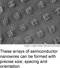
Process orders nanowire arrays
Harvard University researchers have found a way to neatly layer and pattern rows of nanowires.
The method is a step toward using the microscopic wires to build electronics components from the ground up rather than the usual top-down approach of photolithography, which uses light and chemicals to etch components into chips made from semiconductors like silicon.
The researchers used nanowires that were 45 and 90 nanometers in diameter. A nanometer is the span of 10 hydrogen atoms. The arrays could be used to form devices like nanoscale light-emitting diodes and densely-packed computer chips.
The researchers used a previously reported technique to align a layer of nanowires in solution, and formed structures of parallel or crossed nanowires by transferring each layer to a surface, or substrate. They then used photolithography methods to further pattern the nanowire structures into arrays of nanowire field-effect transistors.
The method allows for control of the orientation and spacing of the nanowires, and the orientation, size and spacing of the arrays that form each layer of the structure. This makes it possible to construct practical electronic devices from nanoscale components like nanowires.
The researchers are working on making more complicated arrays,
and ways to interconnect the wires.
Some applications, like nanosensor arrays and large-scale electronic
devices, could be practical within two years, according to the researchers.
The work appeared in the September 10, 2003 issue of Nano Letters.
E-paper closes in on video
Magnetic memory makes logic
Old idea retooled for security
Crystal slows and speeds light
News briefs:
Process orders nanowire arrays
CD writer generates holograms
Nanotubes boost storage
Nanotubes harvest electrons
Bacteria make more electricity
Design enables large neural nets

Research Watch blog
View from the High Ground Q&A
How It Works
RSS Feeds:
News
Ad links:
Buy an ad link
Ad links: Clear History
Buy an ad link
|
TRN
Newswire and Headline Feeds for Web sites
|
© Copyright Technology Research News, LLC 2000-2010. All rights reserved.