Harder chips make more sensitive sensors
By Kimberly Patch, Technology Research NewsA group of researchers from the California Institute of Technology has developed a method of fashioning tiny mechanical parts from silicon carbide, a more durable and more sensitive material than the silicon and gallium arsenide commonly used to make today's computer chips.
Silicon carbide is harder than the other two materials, making it more resistant to wear and more stable at higher temperatures, and thus potentially able to withstand harsher environments. The same trait also gives silicon carbide a higher resonance frequency, meaning it vibrates more times per second. This higher vibration rate enables it to detect subtler changes as a sensor.
"Silicon carbide is a novel semiconductor. It has excellent electrical and mechanical properties. So it was only natural for us to go in that direction and try to make nanoelectromechanical systems out of silicon carbide," said Kamil Ekinci, a postdoctoral scholar at Caltech.
Nanoscale moving parts are designed to avoid contact because the van der Waal's forces between atoms or molecules would make them stick together. A string of 10 carbon atoms would make a line about one nanometer long.
Because the parts of a NEMS device would not touch they would not lose energy due to friction, but they could lose energy due to a similar internal friction action. "The advantage of silicon carbide is that one can chemically treat it and polish it into a robust inert state. This reduces its energy losses and helps keep it operating in a stable manner," Ekinci said.
In addition, the method could be used to make more durable parts for microelectrical mechanical systems (MEMS). The microscale is 1,000 times larger than the nano scale. A red blood cell, at five microns across, is the size of a string of 50,000 carbon atoms. MEMS devices typically include gears, levers and other parts that come into contact with each other.
At this scale there are enough atoms in a part to make the van der Waal's forces negligible, but the effects of friction are stronger than at the macro scale. "Silicon carbide is a strong material and the wear would be less due to friction," Ekinci said.
Although it is obvious that silicon carbide is a very good material because it's very hard, the same trait makes it difficult to work with. To get around this problem, the researchers replaced the usual wet etching process used to make silicon components with a dry etching technique.
They first used photolithography to add electrical contact pads to a wafer of silicon carbide layered on top of silicon. They covered the wafer with a light-sensitive film, exposed the film through a mask, added a layer of gold via thermal evaporation, then dissolved the film so that the gold stuck only to areas patterned by the mask.
Next, the researchers used electron beam lithography to shape individual parts from the wafer. A focused electron beam in an electron microscope wrote patterns on parts of the wafer not protected by a metal mask. They then dry etched the patterns into the material using an ion beam "much like a metal piece is machined in a milling machine," said Ekinci.
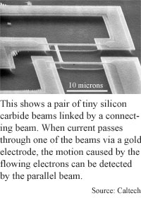
Using this process, the researchers fashioned slivers of silicon carbide that range from 150 to 600 nanometers wide and two to seventeen microns long. The slivers serve as resonators, which are a key component of many types of sensors.
Replacing the wet etching with dry etching is "an experimental breakthrough" said Deepak Srivastra, a senior scientist in computational nanotechnology at the NASA-Ames add caps.
Silicon carbide components are potentially very useful, he added. "[In] high-temperature applications silicon carbide is always better because it's very stable at high temperatures. For some of our [space] applications that is very important."
The material is appropriate to use for resonators because, like silicon and gallium arsenide, silicon carbide is a pure crystal, which makes for efficient vibrations, said Ekinci. "By making the resonator out of a defect-free crystal we can get very low-energy dissipation during the vibration cycle. This is similar to the energy stored in a vibrating spring. If it stores the energy efficiently, it vibrates for a long time," he said.
The small scale of the resonators contributes to their sensitivity. A full-size harp string, for instance, vibrates hundreds of times a second when it is plucked, while the tiny silicon carbide resonators vibrate at millions of times a second, said Ekinci.
Also, because the material is so hard, a sliver of silicon carbide will vibrate at a higher rate than an equivalent size piece of silicon or gallium arsenide. The higher vibration frequencies mean that smaller effects -- like the presence of a small number of atoms interacting with the resonator -- will change the vibration frequency in a way that would not be detectable in a material that was vibrating slower.
"I have done measurements on NEMS resonators where I show only a few thousand atoms [stuck] on the surface create detectable resonance frequency shifts," said Ekinci.
Essentially, the addition of silicon carbide resonators to the general toolbox of electrical components increases the range of resonator frequencies available, said Srivastra. "It's not just high frequency -- you want as broad a range of frequencies that you're able to address at any scale. So by doing this they have [increased the addressable range], and that is good," he said.
Silicon carbide resonators could be used in practical applications in about five years, said Ekinci.
Ekinci's research colleagues were Ya-Tang Yang, Xue-Ming Huang, Larry Schiavone, Michael Roukes from Caltech, and Christian Zorman and Mehran Mehregany at Case Western Reserve University. They published the research in the January 8, 2001 issue of Applied Physics Letters. The research was funded by the Defense Advanced Research Projects Agency (DARPA).
Timeline: 5 years
Funding: Government
TRN Categories: Semiconductors and Materials; Nanotechnology
Story Type: News
Related Elements: Photo; Technical paper, "Monocrystalline Silicon Carbide Nanoelectromechanical Systems," Applied Physics Letters, January 8, 2001
Advertisements:
February 14, 2001
Page One
Quantum effect moves machine
Software speeds gene comparison
Agents learn from traveling salesman
Harder chips make more sensitive sensors
Silver atoms shine red and green
News:
Research News Roundup
Research Watch blog
Features:
View from the High Ground Q&A
How It Works
RSS Feeds:
News
Ad links:
Buy an ad link
| Advertisements:
|
 |
Ad links: Clear History
Buy an ad link
|
TRN
Newswire and Headline Feeds for Web sites
|
© Copyright Technology Research News, LLC 2000-2006. All rights reserved.