Rubber stamp leaves electronic mark
By Eric Smalley, Technology Research NewsProving that old technologies can contribute to contemporary research, a pair of Harvard University researchers has fashioned a high capacity data storage device based on a rubber stamp.
The researchers' electric microcontact printing system can transfer electric charge from the stamp to a thin film of plastic, and can also be used to transfer vanishingly small particles to a surface in the same way photocopiers transfer toner to paper.
The system stamps electric charge into a film of plastic to store about a CD's worth of data in an area 1 centimeter square.
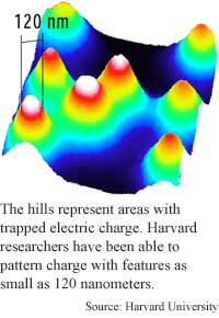
The system can also stamp tiny amounts of particles, including magnetic particles, onto a surface in patterns with features as small as 120 nanometers. Applying particles to surfaces can be used for for high-resolution printing, magnetic data storage and positioning molecules on biological and chemical sensors and testers.
"The organization of small particles and molecules is a difficult task in nanotechnology," said Heiko O. Jacobs, a postdoctoral researcher in the department of chemistry at Harvard University.
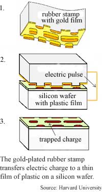
The researchers used photolithography and electron beam lithography to etch patterns on a piece of semiconductor, which then served as a mold for a liquid polymer, said Jacobs. Curing the polymer yielded the rubber stamp. The researchers coated the 5-millimeter-thick stamp with an 80-nanometer gold film.
To write a pattern of charge, the researchers placed the stamp on a negatively-conducting silicon wafer covered with an 80-nanometer film of polymethylmethacrylate (PMMA), which is a plastic that holds electric charge. They applied an electric current to the gold plate of the stamp, which was drawn through the PMMA film to the silicon wafer. The result was an electric charge injected into the areas of the PMMA film in contact with the stamp.
Today's disk drives use the magnetic orientation of microscopic particles to represent bits, but electric charge can also be used to represent bits, said Jacobs. If the charged areas can be made small enough, the technology could become a reasonable alternative to magnetic storage.
A big drawback to previous charge-based data storage technologies has been the difficulty of copying data stored in electric charges. "In charge-based data storage, a rapid replication of data [was] not possible; it took days to pattern data on an area of 1 square inch," said Jacobs. "Electric microcontact printing provides a way to replicate data patterns for charge-based data storage from a master."
The system can transfer a pattern of charge that represents five gigabits of data to the plastic film in about 20 seconds. Five gigabits is 625 megabytes.
Electrets, which are materials that retain electric charges, also have useful optical properties. Electrets can be used to shorten a light wavelength from, for example, red to blue, Jacobs said. Wavelength converters are an essential component of optical telecommunications equipment.
The novelty of electric microcontact printing is not the physics involved, but the demonstration of nanoscale patterned charge transfer, said Aime S. DeReggi, a physicist at the National Institute of Standards and Technology. "It would have some very interesting applications in nanotechnology. The question is how long does the memory remain," he said. "What factors effect longevity? For example, does humidity effect [it]?"
Electric microcontact printing could be used in practical applications in five years, said Jacobs.
Jacobs' research colleague was George M. Whitesides. They published the research in the March 2, 2001 issue of Science. The research was funded by the Swiss National Science Foundation, the German Research Foundation (DFG) and the Defense Advanced Research Project Agency (DARPA).
Timeline: 5 years
Funding: Government
TRN Categories: Data Storage Technology; Semiconductors and Materials
Story Type: News
Related Elements: Technical paper, "Submicrometer Patterning of Charge in Thin-Film Electrets," Science, March 2, 2001
Advertisements:
March 21, 2001
Page One
Net inherently virus prone
Rubber stamp leaves electronic mark
Software spots forged signatures
Magnetic transistor means changeable chips
Filters distill quantum bits
News:
Research News Roundup
Research Watch blog
Features:
View from the High Ground Q&A
How It Works
RSS Feeds:
News
Ad links:
Buy an ad link
| Advertisements:
|
 |
Ad links: Clear History
Buy an ad link
|
TRN
Newswire and Headline Feeds for Web sites
|
© Copyright Technology Research News, LLC 2000-2006. All rights reserved.