Nanotubes
paint clear picture
By
Kimberly Patch,
Technology Research NewsOnce researchers figure out how to manufacture them in bulk, carbon nanotubes could be the key component of large, low-power flat screens that boast resolution higher than the human eye can detect.
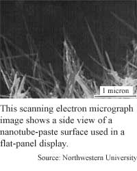
A group of researchers from Northwestern University has built a prototype flat screen that uses nanotubes to direct the photons that light up the screens pixels.
The screen works on the same principle as a standard cathode ray tube (CRT) field emission screen, which uses electrons streaming from a hot filament to light up phosphors on the back of the screen.
Using hundreds of thousands of stationary carbon nanotubes to direct the electrons rather than a filament that rasters, or moves back and forth across the screen 60-80 times per second enables the process to happen at room temperature and from very close to the back of the screen. This makes for a field emission screen that is very thin, very steady, and very high resolution, said Robert Chang, a professor of materials science engineering and director of the materials research Center in Northwestern University.
Nanotubes can do this simply because of the geometry, said Chang. "[Nanotubes] have extremely high aspect ratios -- the tube diameter is always less than about 100 angstroms and the tube length is typically several microns and so it's very easy to put a field on the surface and to extract electrons out of [a nanotube] without having to heat it up," he said.
To make the prototype, which is a one centimeter square, white-on-black screen, the researchers chopped up a batch of nanotubes, mixed them with a paste, and literally painted them on the back of the screen.
To address each pixel, which is made up of hundreds or even thousands of nanotubes, the screen uses the same scheme as today's flat-panel screens -- a grid of wires that turn each pixel on and off. "Each pixel has to have a signal that goes to it. In this case [each pixel] is lots of nanotubes," said Chang. The screen is also low-power; about 15 volts is needed to modulate the pixels, he added. In contrast, a standard CRT requires about 20,000 volts.
Because the nanotube flat-panel works like a CRT by shooting electrons at phosphor it is as bright and can be viewed at as wide an angle as a CRT.
Multiple nanotubes per pixel also makes the screen durable, said Chang. "Because with each pixel you can have thousands of these carbon nanotubes, it's guaranteed redundancy -- the pixel will not deteriorate over time."
And because nanotubes are so small, the number of pixels that can be put on this type of screen could make for higher resolution than the human eye can distinguish. One million of the 10- nanometer nanotubes lined up side-by-side would measure only about a centimeter across. In theory, this type of screen could allow one million times one million pixels per square inch -- a resolution so high there is probably no need for it, said Chang.
Once nanotubes can be manufactured in bulk, the screens would potentially be inexpensive, even for very large screens. "You could make huge screens very cheaply... without expensive lithographic techniques. You just get a roller in the paste and then you just roll it -- this is called screen printing technology. So you can just roll [the paste on a screen] the size of a chalkboard or anything," Chang said.
Demonstrating a field emission screen that is easy to fabricate and uses low control voltages is a significant milestone, said Tsu-Jae King, associate professor of electrical engineering and computer sciences at the University of California at Berkeley, and director of its microfabrication laboratory. "The novelty lies in the development of a simple gated-cathode fabrication process. The resulting cathode array can be operated at low voltages to lower the cost of the display driver chips [and] to lower display power consumption," King said.
The technology could eventually provide a viable alternative to liquid crystal and organic light emitting diode (LED) flat screens for some applications, said King. "I think that field emission display technology has a chance of providing the lowest-cost approach to larger area displays," she said.
The next step is to figure out how to make large quantities of nanotubes, said Chang. "I've got to make kilograms of these nanotubes, [enough to] paint the wall, right? So I'm working feverishly to do that," he said.
This type of screen could be used practically in two years, Chang said.
Chang's research colleagues were Qunhua H. Wang and Min Yan. They published the research in the February, 2001 issue of Applied Physics Letters. The research was funded by the National Science Foundation (NSF).
Timeline: 2 years
Funding: Government
TRN Categories: Semiconductors and Materials
Story Type: News
Related Elements: Technical paper, "Flat-panel Display Prototype Using Gated Carbon Nanotube Field Matters," Applied Physics Letters, February 26, 2001.
Advertisements:
March 28/April 4, 2001
Page One
Programming goes quantum
Diversity trumps fitness
Nanotubes paint clear picture
Hitting the deck cools microdevices
Magnetic fields move microbeads
News:
Research News Roundup
Research Watch blog
Features:
View from the High Ground Q&A
How It Works
RSS Feeds:
News
Ad links:
Buy an ad link
| Advertisements:
|
 |
Ad links: Clear History
Buy an ad link
|
TRN
Newswire and Headline Feeds for Web sites
|
© Copyright Technology Research News, LLC 2000-2006. All rights reserved.