Jolts
yield nanotube transistors
By
Kimberly Patch,
Technology Research NewsScientists from IBM have moved a significant step closer to realizing the dream of using carbon nanotubes as computer chip transistors with a method that allows them to selectively destroy metal nanotubes while leaving those that are semiconducting intact.
Carbon nanotubes, which form naturally when sheets of graphite roll up under high heat and are a component of soot, can be smaller than one nanometer in diameter.
Whether a nanotube conducts electrons freely like a metal or with some resistance like a semiconductor depends on the combination of the angle of the roll and the diameter of the tube.
Commercially made nanotubes are a mix of the two types of tubes, and separating the microscopic cylinders, which naturally stick together in clumps, is a tedious process. The researchers' method of separation is one step toward making nanotubes viable for mass-produced applications.
While studying how much current they could pass through the nanotubes, the researchers found that nanotubes can handle a billion or more amps per square centimeter, or 1,000 times more than copper or aluminum. When they increased the energy of the electrons to about 5 volts, however, the nanotubes started breaking down. "That work... gave us the idea to utilize this destructive event in a constructive manner to actually get rid of the metallic nanotubes," said Phaedon Avouris, manager of nanometer-scale science and technology at IBM's T. J. Watson Research Center.
The researchers have found two distinct uses for metal nanotube destruction. The first is to create an array of semiconducting nanotubes, which has significant implications for eventually using them as transistors on computer chips.
While metallic nanotubes can be used as wires, semiconducting nanotubes can be used as field effect transistors (FETs), which use an electric field to affect whether the device conducts current or not, effectively turning the flow on and off. An array of nanotubes that includes both types, however, means current will always pass through the metallic nanotubes acting as wires, making the semiconducting nanotubes irrelevant. "The metallic nanotubes cannot be affected by the gate, so they're always on," Avouris said.
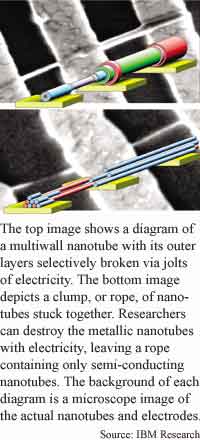
The researchers made an array of semiconducting nanotubes by depositing rope-like clumps of both metallic and semiconducting nanotubes on a substrate, and covering them with electrodes, which they used to stop any current from running through the semiconducting nanotubes. They then identified the shorts, or places where current was passing through metallic nanotubes, and fixed these shorts by applying current strong enough to destroy them. The resulting array consisted of ropes of semiconducting nanotubes connecting pairs of electrodes.
The method is essentially a new way of fabrication that doesn't require separation or orientation of the nanotubes, said Avouris. "We just cover them with electrodes and do the final fabrication by current rather than by chemistry or any other technique," said Avouris.
The researchers have made arrays using several thousand nanotubes and could easily scale that up, said Avouris. "You can make them as big as you want," he said.
The second application for the researcher's method of destroying metal nanotubes is to selectively shape individual multiwall nanotubes, which are essentially nested groups of tubes, by destroying individual tube layers from the outside in.
This allows them to choose the exact diameter of a nanotube, which determines its electrical properties. Using the method, the researchers have fabricated nanotube FET's with bandgaps, or propensity to channel electrons, of their choice. "The bandgap of nanotubes, unlike silicon, is not fixed. It depends on the diameter of the tube. If you start removing [the shells] one by one, the diameter decreases and correspondingly the bandgap increases. So you can stop where you want and you have a transistor with the desired bandgap," Avouris said.
The researchers have also characterized the electrical properties of these transistors, and according to Avouris they are close to those of p-type silicon transistors. P-type transistors use positive holes to carry current, while n-type transistors use electrons.
The nanotube transistor characteristics include contact resistance, meaning how well the nanotubes connect with the electrodes bringing them current, transconductance, which measures how fast the current changes, and mobility, or the ease with which charge carriers move.
The researcher's next steps are to make top-gated transistors, which are the type used in computer chips, and to optimize the transistor characteristics.
Making transistors and arrays using semiconducting nanotubes are significant steps toward eventually making circuits from nanotubes, which have the potential to be more than an order of magnitude smaller than the circuits that make up today's computer chips.
Today's Pentium IV chips, for example, sport about 42 million transistors with features as narrow as 180 nanometers. Computer chips use transistors to form the circuits that perform basic logic functions, and in order to continue to build faster, more powerful computers, chip manufacturers must cram transistors into a smaller space.
Although the lithography techniques used to make these transistors for the past few decades have improved enough to double the number of transistors on a chip every 18 months or so, they're expected to run into the laws of physics within the next decade.
Self-assembled carbon nanotubes are a good candidate to eventually provide transistors small enough to go beyond the lithography size limits.
"Experimentalists already know how to make individual nano-transistors using... single semiconducting nanotubes or other molecules," said Vincent Crespi, assistant professor of physics at Penn State University. The IBM work is "a first step towards practical integration of multiple nano-devices on a single chip. Thats why its important. In the grand scheme of integrated electronics, its only a baby step, but at least the baby has started to walk, he said.
"Its still unclear exactly which techniques of nanoelectronics will pan out into practical devices, Crespi added. "But this work has a reasonable chance, in 10 years, of being seen as one of the important enabling advances for a new technology."
The IBM researchers are "the first group to show a rational approach to making devices out of nanotubes," said Charles Lieber, a chemistry professor at Harvard University. "It's a really nice advance [but] it's going to be pretty hard to scale up," he said.
IBM's destructive method is "another strategy that may help to achieve that next step," toward working nanoelectronics, said Lieber, adding that self assembled materials are another possibility.
Although the IBM process is a step toward working nanoelectronics, it's a long way between nanotube arrays and nanotube logic circuits that can be used in computer chips. Circuits require both p-type and n-type transistors, and lot of work remains to develop large-scale manufacturing processes, making nanotube computer chips likely a decade away, Avouris said.
There's also the possibility of hybrid technologies the use both silicon and nanotubes, he added. "Both silicon and carbon are in the same column of the periodic table and they have many similar properties, so using, for example, nanotubes as interconnects -- metallic wires that connect one device to another -- that's also very promising."
At this point all the work geared toward nanotube circuits is, of course, research, Avouris said. "There are a lot of unknowns... I think as we get closer to 2010 and the end of silicon the pressures to have a working successor will intensify," he added.
Avouris' research colleagues were Philip G. Collins and Michael S. Arnold of IBM's T. J. Watson Research Center. They published the research in the April 27, 2001 issue of the journal Science. The research was funded by IBM.
Timeline: 10 years
Funding: Corporate
TRN Categories: Nanotechnology; Integrated Circuits
Story Type: News
Related Elements: Technical paper, "Engineering Carbon Nanotubes and Nanotube Circuits Using Electrical Breakdown," Science, April 27, 2001.
Advertisements:
May 2/9, 2001
Page One
Jolts yield nanotube transistors
Simulation hints at quantum computer power
Metal makes DNA more conductive
Etching process points to nanotech production
Plastic pins DNA molecules in place
News:
Research News Roundup
Research Watch blog
Features:
View from the High Ground Q&A
How It Works
RSS Feeds:
News
Ad links:
Buy an ad link
| Advertisements:
|
 |
Ad links: Clear History
Buy an ad link
|
TRN
Newswire and Headline Feeds for Web sites
|
© Copyright Technology Research News, LLC 2000-2006. All rights reserved.