Nano-scale plotter goes parallel
By Eric Smalley, Technology Research NewsResearchers at Northwestern University have extended their nanoplotter to support parallel writing tips, paving the way for faster, cheaper development of devices ranging from integrated circuits to DNA analyzers.
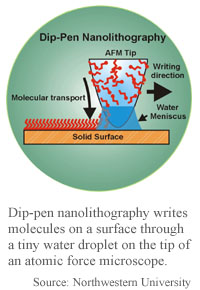
The nanoplotter technology, formally called dip-pen nanolithography, works by dipping the probe tip of an atomic force microscope into an "inkwell" of molecules and using the tip to write on a surface. A tiny water droplet condenses on the tip from moisture in the air, and the ink molecules flow through the droplet to the surface. (see diagram) The device writes lines as fine as thirty molecules wide and one molecule high.
The discovery that varying the pressure on the writing tip didn't change line width enabled the nanoplotter to support parallel pens, said Chad Mirkin, professor of chemistry at Northwestern University. Line width is determined by the size of the water droplet. This means the microscope only needs to monitor one writing tip, even when the nanoplotter uses multiple tips.
The researchers have demonstrated an eight-pen version and are working on a 50-pen version, Mirkin said. In theory, the nanoplotter could be extended to 1,000 pens, he said. The pens are 600 microns apart and the researchers are working on getting them to about 100 microns apart, he said. The team is also working on microfluidic systems for delivering the molecules to the pen tips so they don't have to be dipped.
Because parallel nanolithography is based on the relatively inexpensive atomic force microscope, it will allow many more researchers to produce quantities of nano-scale structures made from a wide range of molecules. "I find that very exciting," said Charles M. Lieber, a professor of chemistry at Harvard University.
Nanolithography technology can be used for making integrated circuits more cheaply than today's electron beam lithography or photolithography, which require expensive equipment and clean rooms. Those technologies also "suffer from [their] serial nature, and while they're very good for making single prototype structures, they're just very time consuming [for] doing a larger scale fabrication," Lieber said.
There's even more opportunity in patterning and building nanometer-scale organic and biological architectures, Mirkin said. "We're getting down to a length scale here where we can literally think about building synthetic antibodies, where you design a pattern that recognizes a particular biomolecule," Mirkin said. "The beauty of it is, with this plotter you don't have to know the best pattern. You can just make thousands of different patterns and ask Which one's best?"
The nanoplotter could be commercially available in 1 to 2 years, according to Mirkin. The project was funded by the U.S. Air Force Office of Scientific Research, the Defense Advanced Projects Research Agency and the National Science Foundation.
Timeline: <2 years
Funding: Government
TRN Categories: Nanotechnology; Semiconductors and Materials
Story Type: News
Related Elements: Diagram; Technical paper in Science, June 9, 2000, p. 1808
Advertisements:
June 28/July 5, 2000
Page One
Cortex chip goes both ways
Sampling ability broadens quantum computing
Nano-scale plotter goes parallel
NASA grasps intricacies of human hand
Algorithm evolves more efficient engine
News:
Research News Roundup
Research Watch blog
Features:
View from the High Ground Q&A
How It Works
RSS Feeds:
News
Ad links:
Buy an ad link
| Advertisements:
|
 |
Ad links: Clear History
Buy an ad link
|
TRN
Newswire and Headline Feeds for Web sites
|
© Copyright Technology Research News, LLC 2000-2006. All rights reserved.