Researchers make cheap telecom laser
By Kimberly Patch, Technology Research NewsAs the world becomes ever more entwined in fiber-optic cable, the race to provide cheap lasers to pulse light down those cables is continuing to heat up.
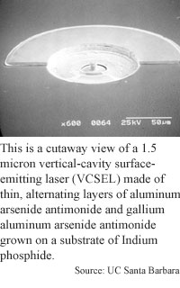
The latest announcement is a 1.55 micron Vertical Cavity Surface Emitting Laser (VCSEL) grown on indium phosphide by researchers from the University of California at Santa Barbara (UCSB).
Because VCSELs are produced in bulk on semiconductor wafers in a single-step process, they are theoretically much cheaper to produce then the edge emitters used commercially today.
The 1.55 micron frequency is one of two most useful for optical communications. It is the frequency where there is the least loss of light signal, and so is most useful for long distances where the use of repeaters to boost signals can be difficult and costly.
A second frequency -- 1.3 microns -- allows for the least amount of dispersion, or spread, of the light signal, which in turn allows more data to be pumped over a line, making it most useful for distances under 30 miles.
The 1.55 micron VCSEL consists of an active region surrounded by electrical contacts, which is in turn sandwiched between a pair of mirrors made up of many layers.
The active region produces light, while the mirror layers act like "a distributed reflector," said Larry Coldren, professor of materials and electrical and computer engineering at UCSB. Each layer of the mirror reflects some light -- maybe 10 percent, he said. The layers are lossless, meaning they pass any light they do not reflect onto the next layer, which does the same. Light generated in the active region intensifies as it bounces back and forth between the mirrors.
The trick to building the 1.55 micron VCSEL was engineering an active region and mirrors with different properties, Coldren said.
The researchers started with indium phosphide because its properties matched what they needed for the active region. To produce the mirrors, they deposited alternating layers of aluminum arsenide antimonide and gallium aluminum arsenide antimonide on the indium phosphide semiconductor substrate. They then etched through the layers into the substrate to make the cavities that are the laser's active regions.
The alternating layers are not latticed matched, or atomically lined up, at every layer, but the layers are engineered so the crystal is latticed matched as a whole, said Coldren. Engineering this strain was the difficult part, he said. "It was basically learning how to grow smooth lattice layers ... that enable the atoms to fit into a perfect single crystal lattice without developing a roughness on the surface."
Another key to the device was putting high conducting thermal and electrical conductivity layers next to the active region where the heat was being generated in order to keep voltage drops low. "That made a tremendous difference," Coldren said.
The researcher's prototype VCSEL has an 800 microamps power threshold, produces just over 1 milliwatt of power in continuous operation and works at temperatures up to 88 degrees Centigrade, according to Coldren.
"Those numbers are very good. It looks like a promising development," said Amnon Yariv, a professor of applied physics at Caltech. The researchers main job now is boosting power, Yariv added. "Today, commercial lasers require 30, 40, 50 megawatts."
The main problem with VCSELs compared to edge emitting lasers is high electrical resistance. The current usually flows through the mirrors, so they therefore... need to put more current through the laser," said Yariv.
Those refinements will take less than a year, said Coldren, who is also chairman and chief technology officer of Agility Communications. Coldren declined to comment on whether Agility, a company in the tunable laser business, has any plans to develop the VCSEL technology.
Coldren's research colleagues were Eric Hall, Shigeru Nakagawa, Guilhem Almuneau, Jin K. Kim and David Buell, all from UCSB. The researchers presented their results at the European conference on optical communications (ECOC) in Munich this September. The work was funded by DARPA.
Timeline: < 1 year
Funding: Government
TRN Categories: Semiconductors and Materials; Telecommunications
Story Type: News
Related Elements: Photo; Technical paper, "88 degrees Celsius, Continuous Wave Operation of 1.55 Micron Vertical Cavity Surface-Emitting Lasers" presented at ECOC in September
Advertisements:
October 18, 2000
Page One
Nanotubes gain larger kin
Quantum computing without weirdness
Pyramid pixels promise sharp pictures
Molecule movement could make memory
Researchers make cheap telecom laser
News:
Research News Roundup
Research Watch blog
Features:
View from the High Ground Q&A
How It Works
RSS Feeds:
News
Ad links:
Buy an ad link
| Advertisements:
|
 |
Ad links: Clear History
Buy an ad link
|
TRN
Newswire and Headline Feeds for Web sites
|
© Copyright Technology Research News, LLC 2000-2006. All rights reserved.