Tiny silicon crystals loom large
By Eric Smalley, Technology Research NewsA technique for growing tiny silicon crystals in orderly rows could eventually give chip makers a means of making circuits and devices several times smaller than current processes allow.
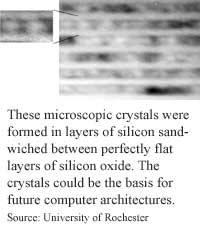
Researchers based at the Nanoscale Silicon Research Initiative at the University of Rochester were able to produce batches of nanocrystals 4.2 nanometers to 50 nanometers in size. A nanometer is a millionth of a millimeter, or about 10 carbon atoms long.
Nanocrystals can serve as quantum dots, which are bits of semiconductor material that can trap small numbers of electrons. Quantum dots are used in tiny lasers, and, in theory, lines of quantum dots could form circuits. Quantum dots are also the basis of several research initiatives to develop new computer architectures.
The technique for producing the nanocrystals is actually a refinement of a basic process used for decades in semiconductor manufacturing. In chip-making, layers of silicon are separated by insulating layers of silicon oxide. The technique for producing nanocrystals focuses on the interfaces between those layers. The key is producing layers of silicon oxide that are atomically flat, resulting in an abrupt interface between the silicon oxide and silicon layers.
There are other techniques for producing silicon nanocrystals, but they are based on "wet" chemistry, said Leonid Tsybeskov, a research scientist at the University of Rochester. "[Our] technique is pure solid fabrication from beginning to end and it's done entirely using standard microelectronic fabrication," he said. "This is the most important difference."
The crystals grow in specific shapes and sizes: rounded 4.2-nanometer crystals, 8.5-nanometer squares, and rectangular measuring 20 by 40 to 20 by 50 nanometers.
The researchers examined the silicon nanocrystals using several methods, including x-ray diffraction and light scattering. "We can prove they're not just crystals, they're not just crystals of the same size, they're not just crystals of the same shape, they're also crystals of the same crystalographic orientation," said Tsybeskov.
Crystalographic orientation is the direction in which the crystals line up. In order to use silicon nanocrystals as quantum dot arrays they have to have the same crystalographic orientation, Tsybeskov said.
"If you could indeed get separate dots that are uniform in size... that would be a very good thing," said Gregory L. Snider, an associate professor of electrical engineering at Notre Dame. "For instance, if you wanted to make memory devices where you're storing single electrons then something like this would be very good," he said.
However, the process could yield nanocrystals that are too closely placed, said Snider. "In an actual electronic device it's not clear to me that these are going to be individual dots," he said.
Producing nanoscale transistors or future computer components using the nanocrystal quantum dots would also require connecting the dots to the outside world. "The most difficult thing is to address each of these dots separately because they're so small," said Tsybeskov.
The researchers hope to connect clusters of the nanocrystals, which should make it possible to use them for transistors and circuits that are several times smaller than those produced using today's photolithography techniques.
"We're talking about something like site-oriented or site-induced formation of dots," said Tsybeskov. "We'll form them not just everywhere but in particular sites where contacts are already waiting for them."
While not as difficult as addressing individual dots, addressing clusters of them is still challenging, said Snider. "Figuring out how to do self-assembled growth where you want it is a difficult problem. For anything other than memory you really have to place the dots accurately," he said.
Although the nanocrystal process could be used now by semiconductor manufacturers to produce arrays of silicon quantum dots, configuring the dots to make useful devices will require other research developments, said Tsybeskov.
The research was published in the September 21, 2000 issue of the journal Nature. Tsybeskov's co-authors were Galina F. Grom and Philippe M. Fauchet of the University of Rochester; David J. Lockwood, John P. McCaffrey and Henri J. Labbé of the National Research Council of Canada; Bruce White Jr. of Motorola Laboratories; and Joachim Diener, Dmitri Kovalev and Fred Koch of the Technical University of München in Germany.
The research was funded by the Army Research Office, the National Science Foundation, the Semiconductor Research Corporation, Motorola Inc. and Advanced Micro Devices Inc.
Timeline: Now; Unknown
Funding: Government; Corporate
TRN Categories: Semiconductors and Materials
Story Type: News
Related Elements: Photo; Technical paper "Ordering and self-organization in nanocrystalline silicon" in September 21, 2000 Nature
Advertisements:
November 8, 2000
Page One
Electronics link mind and body
Chip promises faster light-to-circuit link
Coffee effect could benefit circuit connections
Tiny silicon crystals loom large
Switch offers cheap local-long distance link
News:
Research News Roundup
Research Watch blog
Features:
View from the High Ground Q&A
How It Works
RSS Feeds:
News
Ad links:
Buy an ad link
| Advertisements:
|
 |
Ad links: Clear History
Buy an ad link
|
TRN
Newswire and Headline Feeds for Web sites
|
© Copyright Technology Research News, LLC 2000-2006. All rights reserved.