Holey chips channel light
By Kimberly Patch, Technology Research NewsLaser beams have traditionally been guided in three dimensions by the atomic structure of crystals. But taking the crystal guides down a dimension may point the way to cheaper, lower power light guides and even light-switched computer chips.
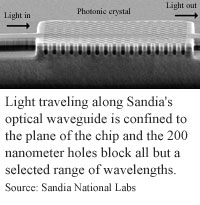
Similar projects at Sandia National Laboratories and Kyoto University are aiming to do this using tiny bars studded with many precise holes. The physical characteristics of these flat, pockmarked crystals guide the light in just two dimensions -- along the plane of the bar. But the high refractive index of the materials that make up the bars prevents light from escaping into the third dimension -- the top and bottom surface of the bar.
The refractive index is a measure of how much a transparent substance bends light. It is the phenomenon that distorts the appearance of an object spanning water and air.
Key to the usefulness of these waveguides is their flexibility. The size and placement of the holes can be changed, or tuned, to guide wavelengths of light at different frequencies, including those useful to the telecommunications industry.
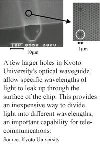
The Sandia team's bar is a sandwich of silicon oxide, gallium arsenide, and aluminum oxide. The Kyoto team's structure is made of indium gallium arsenide phosphate and indium phosphate. Using electron beam lithography and reactive ion etching, the researchers put the tiny layers together and punched them full of holes about 200 nanometers across.
The holes are about one tenth the size of an E. Coli bacteria. The size and placement of the holes block light in all but a selected band of wavelengths. The holes essentially mimic the electron placement in an atom that enables certain wavelengths of light to glide between the atoms of a crystal.
The Kyoto team took their research a step further, showing that the device can be used to trap, then emit single photons. To do this, the team added slightly larger holes, or defects, to the structure, which allowed photons of a specific wavelength to leak vertically from the surface of the device.
"We reached the idea to utilize this leaky property of the 2D photonic crystal slab to obtain a new function...trapping and emission of photons by a single defect," said Susumu Noda, a professor of electronic science and engineering at Kyoto University. "Once the photons are trapped and confined in a tiny cavity formed by [this] defect, [they] should leak out into the vertical direction."
This ability could be exploited for wavelength division multiplexing (WDM) -- dividing light into bands of slightly different wavelengths. This is a valuable trait for telecommunications because it enables more than one signal at a time to travel over a single fiber strand and still be differentiated at the other end.
"[They] took the further step of making something that was functional," said Eli Yablonovitch, an electrical engineering professor at the University of California at Los Angeles. "They ran an optical signal down a channel [without holes that was] acting like a wire for lightwaves. Cavities adjacent to that wire... would then pick up only certain wavelengths from the main channel and couple them up vertically, and so it was performing the wavelength division multiplexing function," said Yablonovitch.
The devices are potentially very cheap simply because they are so very small -- about 1/10,000th the size of standard telecommunications lasers, according to Noda. "Generally speaking, cost goes with size," said Yablonovitch. "If you have a very tiny component you can punch very large quantities out of a wafer and therefore the cost is terribly low."
There are several steps to go through before these devices can be put to any practical use, however. First, there is work to be done in figuring out how to manufacture devices with such tiny holes, said Yablonovitch.
"You have to show that you can actually manufacture it with the required precision," he said. "Then you have to figure out how to do the switching. Probably the most difficult [problem] is how to get the light in and how to get the light out. Neither of these [waveguides] are very efficient. That's the biggest challenge. I think if we can solve that then probably the rest of it would just fall into place, said Yablonovitch.
The Kyoto team's next step is a defect engineering study that will further explore the effects of adding larger holes, or defects, into the device, said Noda. "If we change the defect feature -- not only size but also effective refractive index -- various characteristics of the device such as coupling efficiency [will be] drastically changed."
The device can also be used as a switch, or circuit, by enabling it to dynamically change its refractive index, said Noda. The Kyoto team has figured out how to do this, and is filing for a patent, he said.
In theory, optical switches made with these perforated devices would be both cooler and faster than current versions and could eventually provide an alternative to today's computer chips. "The extremely low loss nature of light-guiding and bending in a photonic crystal implies less heating," said Lin. Optical switches would be faster both in terms of the time it takes for a signal to travel and because very broad bandwidths are possible, Lin added.
It will take another two or three years to make a practical WDM device, and five years to make an optical circuit, said Noda.
Next for the Sandia team is making 2D photonic crystals that work at the 400-700 nm blue and red visible light wavelength range and adding a gain medium to the devices to make them more efficient, said Shawn Lin, a member of the technical staff at Sandia National Labs. The team is also working on figuring out how to use the devices for optical switching, he said.
Two-dimensional photonic crystals could be used practically in two to five years, said Lin.
Noda's research colleagues were Alongkarn Chutinan and Masahiro Imada of Kyoto University. They published their research in the October 5, 2000 issue of Nature. The work was funded by the Japanese Ministry of Education, Science and Culture and by the Japan Science and Technology Corp. (JSP).
Lin's research colleagues were Edmond Chow, J. R. Wendt, W. Zubrzycki, H. Hou, and A. Alleman of Sandia National Laboratories, and S. G. Johnson, P. R. Villeneuve and J.D. Joannopoulos of the Massachusetts Institute of Technology (MIT). The work was funded by the Department of Energy (DOE).
Timeline: Kyoto University project: 2-3 years, 5 years; Sandia project: 2-5 years
Funding: Kyoto University project: Corporate, Government; Sandia project: Government
TRN Categories: Optical Computing, Optoelectronics and Photonics
Story Type: News
Related Elements: Technical paper, "Trapping and Emission of Photons by a Single Defect in the Photonic Bandgap Structure," Nature, October 5, 2000. Technical paper, "Three-dimensional Control of Light a Two-dimensional Photonic Crystal Slab," Nature, October 26, 2000
Advertisements:
November 22, 2000
Page One
Holey chips channel light
Piezoelectric sliver forms sensor
Self-tuning software speeds networks
Software cross-sorts gene data
Electron beams turnout tinier tubes
News:
Research News Roundup
Research Watch blog
Features:
View from the High Ground Q&A
How It Works
RSS Feeds:
News
Ad links:
Buy an ad link
| Advertisements:
|
 |
Ad links: Clear History
Buy an ad link
|
TRN
Newswire and Headline Feeds for Web sites
|
© Copyright Technology Research News, LLC 2000-2006. All rights reserved.