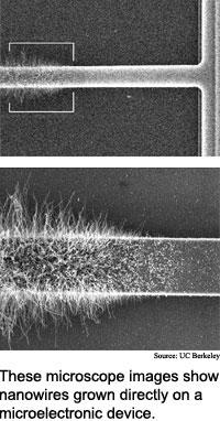
Process puts nanotubes in place
University of California at Berkeley researchers
have found a way to grow silicon nanowires and carbon nanotubes directly
on delicate microelectronic components.
The simple method promises to enable vanishingly small, relatively
inexpensive gas detectors, pressure sensors, biosensors and strain gauges
that monitor structures like airplane wings, according to the researchers.
The method could also eventually foster components for nanoelectronics
and for quantum computers, which are theoretically many orders of magnitude
faster than today's computers.
The researchers used a vacuum and resistive heating -- the warming
technology ordinary toasters employ -- to provide the 700 to 1,100 degrees
Celsius temperatures needed to form nanowires and nanotubes from a metal
catalyst and chemical vapor. The heating was restricted to a bridge structure,
keeping nearby electronic components a safe 25 degrees. Nanowires or nanotubes
formed depending on the temperature, catalyst and vapor used.
The researchers made nanowires 30 to 80 nanometers in diameter and
up to 10,000 nanometers long, and nanotubes 10 to 15 nanometers in diameter
and up to 5,000 nanometers long. A nanometer is one millionth of a millimeter,
or the span of 10 hydrogen atoms.
Simple sensors could be built within a year, and the method could
be used commercially within ten years, according to the researchers. The
work appeared in the June 30, 2003 issue of Applied Physics Letters.
DNA makes nano barcode
Study reveals Net's parts
Recommenders can skew results
Light pipes track motion
News briefs:
Material helps bits beat heat
Process puts nanotubes in place
Printing method makes biochips
Tiny T splits light
Tiny walls sprout nanowires
Big sites hoard links

Research Watch blog
View from the High Ground Q&A
How It Works
RSS Feeds:
News
Ad links:
Buy an ad link
Ad links: Clear History
Buy an ad link
|
TRN
Newswire and Headline Feeds for Web sites
|
© Copyright Technology Research News, LLC 2000-2010. All rights reserved.