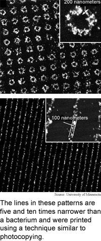
Process prints nanoparticles
One of the challenges of nanotechnology is finding ways to position the minuscule building blocks that make up microscopic electronics and machines.
Researchers from the University of Minnesota have coaxed tiny particles of gold, silver and carbon to assemble into patterns on silicon wafers over areas as large as a square centimeter by using electrical charge patterns to attract and position the nanoparticles.
The process, which uses the same principle as photocopying, can eventually be used to form wires, circuits and even nanoscale devices like transistors and lasers, according to the researchers.
The researchers were able to print 10- to 100-nanometer particles into patterns with features as fine as 200 nanometers using a process that started with the nanoparticles suspended in liquid. They were able to print features as fine as 100 nanometers by directing particles towards the charged surface using gas.
A nanometer is the span of 10 hydrogen atoms, and 100 nanometers is 1,000 times narrower than a human hair.
The process can handle many types of materials, can print patterns
quickly by using parallel print heads, and has the potential to print
as narrow as 10 nanometers, according to the researchers.
The technique is several years away from being used in practical
production processes, according to the researchers. The work appeared
in the October, 2003 issue of Nanotechnology.
Body network gains speed
Queries guide Web crawlers
Nanowires make flexible circuits
DNA forms nano waffles
Briefs:
Fiber handles powerful pulses
Process prints nanoparticles
Single electrons perform logic
Embedded rotors mix fluids
Nanowires boost plastic circuits
Chip mixes droplets faster

Research Watch blog
View from the High Ground Q&A
How It Works
RSS Feeds:
News
Ad links:
Buy an ad link
Ad links: Clear History
Buy an ad link
|
TRN
Newswire and Headline Feeds for Web sites
|
© Copyright Technology Research News, LLC 2000-2010. All rights reserved.