Nanowires make flexible circuits
By
Eric Smalley,
Technology Research NewsElectronics have been made from silicon chips since vacuum tubes began fading into history in the '60s. Nanotechnology could be the key to the next big shift.
Chip-making processes use light and chemicals to etch microscopic components into wafers of semiconductors like silicon. The next wave of electronics is likely to feature microscopic circuits built on or into all manner of materials. These new circuits could be constructed from nanoscale components made en mass via quick, relatively cheap chemical self-assembly.
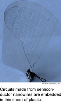
Researchers from Nanosys, Inc. have found a way to assemble large arrays of nanowires made from silicon or other semiconductors into a densely-packed thin film, then process the assembly to produce relatively efficient transistors on a variety of surfaces.
The technology may eventually enable very large flat-panel displays, tiny radio frequency identification devices, and disposable computing and storage electronics, said Xiangfeng Duan, an advanced technology scientist at Nanosys.
The process that attaches the arrays to a surface can be carried out at room temperature, which makes it possible to put transistors on a wide array of cheap and useful surfaces, including glass, textiles, plastic and even paper, said Duan. Making the semiconductor nanowires, which requires high temperatures, is carried out before the components are applied to the surface.
The researchers attached the 20- or 40-nanometer-diameter silicon nanowires by suspending them in a liquid and then flowing the liquid across a surface. This causes the nanowires to align in one direction and form a thin film. The researchers then use conventional photolithography to put electrodes on the nanowire film, forming arrays of transistors.
The process promises to enable electronics that can be spread cheaply over large areas. It can be used to apply virtually any semiconductor material to virtually any substrate, said Duan. The nanowire thin film could eventually be spread on surfaces using low-cost techniques like inkjet printing, he said.
The Nanosys researchers aim is to use nanoscale electronic components to construct cheaper large-scale electronics, said Duan. "From the outset, we have [exploited] nano materials not for electronic miniaturization, but for better and cheaper electronics over large areas," he said.
The researchers produced a prototype of thin film transistors on a plastic substrate and showed that it was relatively efficient, according to Duan. Each transistor is made up of a group of nanowires that channels electric current, and titanium-gold electrodes that brings current into and out of the device.
Transistors carry out the logic of computing. They can be switched on or off and so can carry a signal or no signal. The presence of an electrical signal can represent a 1 and the absence of a signal a 0.
Regular transistors are etched into the surfaces of relatively expensive crystalline silicon wafers. Thin film transistors, which can be mounted on various surfaces, are usually made from amorphous silicon, polycrystalline silicon or organic materials.
The atoms of crystalline silicon are arranged in an orderly lattice structure. Polycrystalline silicon is an aggregation of tiny silicon crystals. Crystalline silicon conducts electricity more efficiently than polycrystalline silicon because there are no crystal grain boundaries to slow electrons. The atoms of amorphous silicon are unordered, which makes it a relatively poor conductor. Similarly, electrons travel across the molecules of organic materials less efficiently than across the atoms of a crystal.
Though the researchers' thin film is not crystalline, the nanowires themselves are. "Nanowire thin film transistors have a perfect conducting channel formed by multiple single-crystal nanowire paths -- like a log bridge -- in parallel," said Duan.
The researchers prototype had a carrier mobility of 119 centimeters squared per volt second, which is similar to the highest reported performance for polycrystalline silicon electronics, according to Duan. Amorphous silicon and organic electronics typically have carrier mobilities of less than 1 cm per volt second, he said. Mobility is a measure of the velocity of charge carriers in a device, and determines the size of transistor current and the switching speed of the device.
The researchers also demonstrated that cadmium sulfide nanoribbons can also be used to produce thin film transistors. "Our concept of using nanowires or nanoribbons for macro electronics [is appropriate] for a broad range of materials," said Duan.
The researchers' process "can be implemented in production scale with currently available or foreseeable technologies," said Duan.
Duan's research colleagues were Chunming Niu, Vijendra Sahi, Jian Chen, J. Wallace Parce, Stephen Empedocies and J. L. Goldman from Nanosys. The work appeared in the September 18, 2003 issue of Nature. The research was funded by Nanosys.
Timeline: Now
Funding: Corporate
TRN Categories: Materials Science and Engineering; Nanotechnology
Story Type: News
Related Elements: Technical paper, "High-performance Thin-Film Transistors Using Semiconductor Nanowires and Nanoribbons," Nature, September 18, 2003
Advertisements:
October 22/29, 2003
Page One
Body network gains speed
Queries guide Web crawlers
Nanowires make flexible circuits
DNA forms nano waffles
Briefs:
Fiber handles powerful pulses
Process prints nanoparticles
Single electrons perform logic
Embedded rotors mix fluids
Nanowires boost plastic circuits
Chip mixes droplets faster
News:
Research News Roundup
Research Watch blog
Features:
View from the High Ground Q&A
How It Works
RSS Feeds:
News
Ad links:
Buy an ad link
| Advertisements:
|
 |
Ad links: Clear History
Buy an ad link
|
TRN
Newswire and Headline Feeds for Web sites
|
© Copyright Technology Research News, LLC 2000-2006. All rights reserved.