Crossed nanowires make Lilliputian LEDs
By Kimberly Patch, Technology Research NewsOne of the challenges of making nanoscale components is dealing with the atomic forces that don't generally affect parts at the macro -- or even micro -- scales. Another challenge is simply assembling the tiny parts.
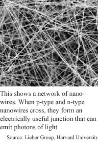
A group of researchers from Harvard University have made nanoscale light emitting diodes (LEDs) just by crossing two types of nanoscale wires made from indium phosphide.
The group physically crossed the wires using two distinct methods. The first uses electric fields to snap wires into place one by one. A second, more scalable method controls the flow direction of a fluid containing the wires to make multiple connections on multiple wires. "We've made some fairly complex structures and multiple junctions," using the flow method, said Charles Lieber, a chemistry professor at Harvard.
Arrays of LED junctions could eventually be used to image cellular-scale objects, to detect chemicals at that scale, to induce photochemical reactions on a gene chip, or as optical interconnects in an electrical circuit, Lieber said. The idea is to eventually make electronic circuitry from these building blocks, he said. "We'll see how far we can push this in terms of actually making integrated structures."
The wires range from 5 to 20 nanometers in diameter and 10 to several hundred microns long. The two types of wire are doped, or augmented, with different materials to give them different electrical properties. An n-type wire uses negatively charged electrons to carry current. A p-type carries current using a positive charge, or holes. "You can make these basic devices by just simply crossing p- and n-type wires and that makes a p-n junction," Lieber said.
Once the researchers get the wires to touch, they stick together. "It's just the interaction of a van der Waals' type of reaction with the surface," said Lieber. Van der Waal's force is a relatively weak force that comes into play when atoms or molecules are close to each other. It gets stronger as atoms or molecules grow closer, and is enough of an attraction to make nanoscale objects stick together.
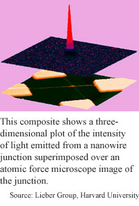
The junctions made by crossing these two types of wires emit light. Because the wires are small enough to show quantum effects, the diameter of the wire changes the size of the lightwave, and thus the color of the light. "Different diameters emit different color lights because of the quantum confinement in the wires," said Lieber.
The researchers have shown a color range of about 700 to 900 nanometer wavelengths using the indium phosphide wires. These wavelengths are in the red and infrared range.
By pairing the wire size effect with wires made of different materials, nanowire LEDs could span the whole range of the visible spectrum of light, said Lieber. "We could go then from indium phosphide to gallium arsenide to cover the midrange -- red and green colors -- and then you could use gallium nitride to go into the blue, which is what we're working on now but we don't have any real results yet," he said.
The group is also working on making the LEDs more efficient. The group's LEDs converted only one percent of the electricity flowing through the wires to light, while commercial red LED's, for instance convert around 50 percent. "There's a lot of basic, basic science that has to be done to... improve the efficiency," said Lieber.
The research covers the key elements for building nano circuitry, said Yue Wu, an assistant physics professor at the University of North Carolina. "They have the [nanoscale] building blocks, they show they have junctions, and they show not only the electrical behavior but also the optical property... you get light out of the junction, he said. "These are the crucial elements for making optoelectronic devices based on nanoscale materials."
The field is still young, making it difficult to predict eventual commercial potential, said Wu. For example, the physics of the p-n junction made of crossed wires are slightly different from conventional junctions because the two wires are not fused together. This different type of p-n junction, however provides "a current-to-voltage characteristic that looks exactly the same as what you would expect from a conventional p-n junction," he said.
In the end, "since it's very promising in terms of reproducing all the familiar characteristics that we know from current semiconductor devices, there's bound to be huge potential," said Wu.
The first practical applications for nanowire arrays will likely be sensing and imaging; these types of applications could show up in one or two years, said Lieber.
Lieber's research colleagues were Xiangfeng Duan, Yu Huang, Yi Cui and Jianfang Wang of Harvard. They published the research in the January 4, 2001 issue of Nature. The research was funded by the Office of Naval Research and the Defense Advanced Research Projects Agency (DARPA).
Timeline: 1-2 years
Funding: Government
TRN Categories: Semiconductors and Materials; Integrated Circuits; Nanotechnology
Story Type: News
Related Elements: Photo, Technical paper, "Indium Phosphide Nanowires as Building Blocks for Nanoscale Electronic and Optoelectronic Devices," Nature, January 4, 2000
Advertisements:
January 17, 2001
Page One
Light spins resin rotors
Crossed nanowires make Lilliputian LEDs
Simulation sizes up Web structure
Quantum bit hangs tough
Sowing strain reaps ordered dots
News:
Research News Roundup
Research Watch blog
Features:
View from the High Ground Q&A
How It Works
RSS Feeds:
News
Ad links:
Buy an ad link
| Advertisements:
|
 |
Ad links: Clear History
Buy an ad link
|
TRN
Newswire and Headline Feeds for Web sites
|
© Copyright Technology Research News, LLC 2000-2006. All rights reserved.