Chemists
concoct tiny lasers
By
Eric Smalley,
Technology Research NewsOne way to cram more data onto compact discs and through fiber-optic channels is to use shorter lightwaves. Ultraviolet light is about half the wavelength of the red light generated by the lasers in many commercial devices, and, unlike still shorter x-rays, ultraviolet light can be controlled with lenses and mirrors.
The trick is to find suitable materials and techniques for making ultraviolet lasers that are small enough to be built into semiconductor devices.
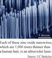
Researchers at the University of California at Berkeley have taken a big step in that direction by growing microscopic forests of vertical nanowires; each is a laser 1,000 times narrower than a human hair.
The nanowires emit ultraviolet laser light when they are pumped by another laser, according to Peidong Yang, an assistant professor of chemistry at Berkeley.
When a material is pumped with energy, the electrons of its atoms move to a higher energy state. When the electrons return to their low-energy states they release the excess energy, often in the form of light.
Lasers work by bouncing this emitted light between two mirrors that are positioned to send the light back and forth through the material. The reflected light adds to the original energy source to produce yet more emitted light, which in turn bounces between the mirrors. This feedback increases the intensity of the light and results in a laser beam.
Semiconductor lasers, which are widely used in communications networks and data storage devices, are a sandwich of three layers of semiconductor. The middle layer is the amplification medium and the outer layers are the mirrors. Electric current provides the initial energy.
Each nanowire is a laser because its ends are sharply defined, which allows them to serve as mirrors that bounce light back and forth along the length of the nanowire. "The [top] end is almost atomically sharp," said Yang.
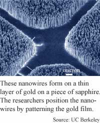
The nanowires are grown by wafting a vapor of zinc oxide over a sapphire chip that is coated with a thin film of gold. Most of the nanowires are within 70 to 100 nanometers in diameter, according to the researchers. The nanowires grow at a rate of about one micron per minute, and the researchers have made nanowires 2 to 10 microns tall.
The crystal structure of the sapphire substrate causes the nanowires to grow in a precise shape, said Yang. "In general, there are lots of methodologies [for growing] nanowires. It's really a matter of growth control, with careful control of the substrate," he said.
The gold film serves as a catalyst for nanowire growth, so putting it on the sapphire substrate in a particular pattern causes the nanowires to grow in that pattern, said Yang. "We can purposely put these nanowire lasers at a particular place, depending on where we put the catalyst," he said.
The major hurdle to developing practical ultraviolet nanowire lasers is figuring out how to produce the lasing action using electricity rather than another laser. "We demonstrated... this optically-pumped laser. If we can successfully put this device into electron injection configuration, then it immediately can be commercialized," said Yang.
The researchers are also working on changing the chemical composition of the nanowires to slightly altered the light wavelengths the lasers emit. "We're working on tuning the composition of the systems so that we can tune the wavelengths... from blue to deep UV," said Yang.
In addition to communications and data storage, nanowire lasers on labs on a chip could be used for spectroscopy, said Yang. Spectroscopy is a method of using light to determine the chemical composition of a substance.
The nanowire lasers could be used in practical applications in five to ten years, said Yang.
Yang's research colleagues were Michael H. Huang, Haoquan Yan, Yiying Wu and Hannes Kind of the University of California at Berkeley, and Samuel Mao, Henning Feick, Eicke Weber and Richard Russo of Lawrence Berkeley National Laboratory. They published the research in the June 8, 2001 issue of the journal Science. The research was funded by the Camille and Henry Dreyfus Foundation, 3M Corporation, the National Science Foundation (NSF), the Department of Energy and the University of California at Berkeley.
Timeline: 5-10 years
Funding: Private, Corporate, Government, University
TRN Categories: Materials Science and Engineering; Optical Computing, Optoelectronics and Photonics
Story Type: News
Related Elements: Technical paper, "Room-Temperature Ultraviolet Nanowire Nanolasers," Science, June 8, 2001
Advertisements:
June 27, 2001
Page One
Chemists concoct tiny lasers
Slimmer chips handle fast nets
Prototype transistors promise speedy chips
Molecules make short-term memory
Micromachine parts relax into place
News:
Research News Roundup
Research Watch blog
Features:
View from the High Ground Q&A
How It Works
RSS Feeds:
News
Ad links:
Buy an ad link
| Advertisements:
|
 |
Ad links: Clear History
Buy an ad link
|
TRN
Newswire and Headline Feeds for Web sites
|
© Copyright Technology Research News, LLC 2000-2006. All rights reserved.