Bendable nanotubes store bits
By Eric Smalley, Technology Research NewsOne of the first steps to building blazingly fast, dirt cheap and vanishingly small molecular computers is figuring out how the devices would hold data.
Carbon nanotubes have looked like ready-made microscopic wires to researchers for long time, and the idea of building memory arrays from perpendicular strands of them is nothing new. One of the challenges, however, has been figuring out how to control the junctions where the wires cross in order to create the on and off states necessary for binary computing. Most approaches have focused on inserting spring-like molecules between the crossed nanotube wires.
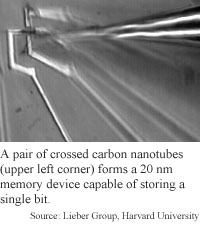
A different approach that uses the mechanical properties of carbon nanotubes has paid off for researchers at Harvard University who have built a tiny memory device that could be a predecessor to the building blocks of tomorrow's molecular computers.
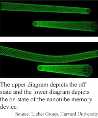
The Harvard team coaxed the nanotubes into making and breaking the connections on their own. Carbon nanotubes come in two forms: semiconducting and metallic. Metallic nanotubes will bend toward a perpendicular semiconducting nanotube when electrically charged. When a metallic nanotube is one to two nanometers away from a semiconducting nanotube, the electrical resistance at the junction is low, creating an on state. When the nanotubes are apart the resistance is much higher, creating an off state.
"The clever thing is it combines both electronic and mechanical properties of single-wall nanotubes," said Yue Wu, an associate professor in the physics and astronomy department at the University of North Carolina, Chapel Hill. "It gives people hope to make large [memory] arrays. It -- to a certain extent -- has demonstrated experimentally that this can be done."
Because carbon nanotubes are so small, little more than a nanometer in diameter, memory arrays built from them could house 1012 cross-wire elements per square centimeter. That would be 10,000 to 30,000 times more dense than today's Dynamic Random Access Memory (DRAM) memory chips, said Charles M. Lieber, professor of chemistry at Harvard and leader of the team that developed the nanotube technique.
"It's much higher density than will ever be attainable with silicon [wafer] technology," he said. In principle these memory arrays could also be 1,000 to 10,000 times faster than today's memory chips, he added.
Perhaps as significant as the scale of Harvard's nanotube memory device is its ability to remain in either the on or off state without a continuous electrical charge. Most computer memory today only works when the computer is on because it needs to be continuously refreshed. Non-volatile silicon wafer memory exists, but it is much less dense than standard computer memory.
Carbon nanotube arrays could also be used to build computer processors. "We think in the longer term actually making a computer almost entirely based on this type of architecture is a possibility," Lieber said. "They certainly offer the promise of a lot more power. [And realizing] the potential of the assembly approaches that we and other people are using it's going to be low cost."
However, there are several hurdles to overcome before anyone is going to be able to produce memory modules from carbon nanotubes.
"The distance between the crossed wires has to be controlled fairly precisely, from one to two nanometers," Wu said. "You have to come up with a way that you can assemble many, many of these cross-wires. To make this pattern of nanotubes with precise control of distance -- that's going to be the difficulty. The other difficulty right now [is] when people grow nanotubes, we all grow spaghetti. How to grow straight tubes, that's also something people need to work on."
In addition, there is not yet a reliable way to produce separate sets of metallic and semiconducting nanotubes. The Harvard team is working on a way around this problem by using silicon wires for the semiconducting portion of the array, Lieber said. However, this will not produce the same density as a purely nanotube array, he said.
A silicon wire-carbon nanotube hybrid memory array could become commercially viable in about two years, according to Lieber. Barring an earlier breakthrough of being able to build separate semiconducting and metallic nanotubes, purely nanotube memory arrays are five to 10 years away, he said
The research was funded by the Defense Advanced Research Projects Agency and the Office of Naval Research. The Harvard team reported on their findings in a paper in the July 7 issue of the journal Science.
Timeline: >2; >5
Funding: Government
TRN Categories: Nanotechnology; Data Storage Technology; Integrated Circuits
Story Type: News
Related Elements: Technical paper "Carbon Nanotube-Based Nonvolatile Random Access Memory for Molecular Computing" in July 7 Science
Advertisements:
July 12, 2000
Page One
Bendable nanotubes store bits
Protein-coated chip sniffs out bacteria
The little light-sensitive molecule that could
Fault-tolerant free speech
Chemical reaction zips nanowires onto silicon
News:
Research News Roundup
Research Watch blog
Features:
View from the High Ground Q&A
How It Works
RSS Feeds:
News
Ad links:
Buy an ad link
| Advertisements:
|
 |
Ad links: Clear History
Buy an ad link
|
TRN
Newswire and Headline Feeds for Web sites
|
© Copyright Technology Research News, LLC 2000-2006. All rights reserved.