Electron
beam welds nanotubes
By
Ted Smalley Bowen,
Technology Research NewsOne of the keys to getting carbon nanotubes to work as miniscule circuits is finding a way to connect them together that doesnt squash them or alter the way they conduct electrical current.
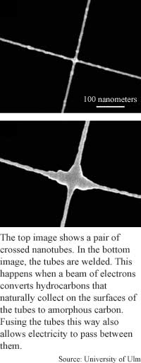
A researcher at the University of Ulm in Germany has found a way to solder nanotubes by shooting a beam of electrons at the hydrocarbon atoms that build up on the tubes' surfaces. This both connects the tubes and transforms the hydrocarbons, which are insulators, into a material that conducts electricity.
The process produces a clump of bonding material at the junctions of the tubes without melting the tubes into each other. Because the resulting connections are made to the outer surfaces of the nanotubes, they are expected to provide better conductivity than welded joints.
Zapping the tubes with a beam of electrons from an electron microscope fixes the superficial, shifting hydrocarbon atoms in place, according to Florian Banhart, a lecturer at the University of Ulm. The electrons also change the insulating hydrocarbons into amorphous carbon and its graphitic cousin, which are conductors, he said.
Hydrocarbons in the air are attracted to carbon nanotubes at room temperature. Over time, enough of the normally unwanted hydrocarbon contamination accumulates to provide a sort of proto-solder on the surface of the nanotubes. Nanotubes can be smaller than one nanometer in diameter. A nanometer is one millionth of a millimeter, or about 10 carbon atoms long.
In his experiments, Banhart worked with grids of nanotubes that were aged several hours to several years. The longer the tubes were exposed to the air, the more hydrocarbons they had, resulting in more solder.
The soldering method could benefit both electronic and semiconductor development, according to Banhart. Nanodevices have to be connected by conductive wires. Nanotubes [that] are conductive like metals... can be used as nanowires much like cables or strip conductors in today's electronics. Semiconducting [nanotubes can] be used as building blocks of devices [such as] diodes, transistors etc. In each case, tubes have to be connected with their periphery and with each other, he said.
Banhart soldered the junctions of nanotubes placed on a platform within the lens of a scanning electron microscope (SEM). This microscope configuration allowed him to focus the beam with a resolution finer than one nanometer.
Once the tubes were soldered securely, Bernhard used a higher SEM voltage to change the amorphous carbon to graphitic carbon.
Graphitic carbon is more conductive than amorphous carbon, which makes it worthwhile to change the solder. Amorphous carbon can be converted to graphitic carbon using a beam of electrons of a higher energy from a tunneling electron microscope (TEM), or through annealing in a furnace.
The tunneling electron microscope irradiation method is probably more appropriate than annealing, said Banhart. We expect that annealing would lead to better graphitization if temperatures above 1,000°C are used. But such high temperatures would not be applicable in device technology. We believe that graphitization by irradiation is the better technique because this could be done in the same machine as the soldering and without [heating] material, he said.
While Banhart used hydrocarbon build-up that occurred through exposure to air, coating the tubes with hydrocarbons or polymeric material could be added to the nanotube fabrication process, he said.
The types of electrical contacts the soldering forms and the levels of conductivity it produces have not yet been measured, according to Banhart.
A technique for connecting the tubes is needed before the soldering technique can be applied commercially, said Banhart. "First, it would be necessary to arrange the tubes in such a way that devices can be created. This is certainly the more difficult challenge. The soldering in an electron beam could then be carried out in an apparatus such as used for electron beam lithography, he said.
Commercial application of the soldering technique could be feasible as soon as nanotubes are applied on a large scale in technology, maybe in a couple of years, said Banhart.
This work provides a detailed roadmap for investigating the use of carbon 'solder' to make robust, mechanically stable electrical connections between nanotubes," said James Hone, a researcher at the California Institute of Technology. "[It] builds on previous work in which nanotubes were attached to AFM tips in a similar way. I think the main advances described by [Banhart] are the technique used for the first time to make junctions between nanotubes, and used at smaller scales than before, he said.
"The next step will be to measure the electrical conductivity of nanotube junctions produced by this technique," said Hone. "If these junctions prove to be highly conducting, then it might be possible to fabricate larger-scale integrated circuits from arrays of nanotubes by this soldering technique."
Banhart described his work in a technical paper published in The American Chemical Societys Nano Letters, June, 2001. The research was funded by the University of Ulm.
Timeline: > 2 years
Funding: nbsp; University
TRN Categories: Nanotechnology; Semiconductors and Materials
Story Type: News
Related Elements: Technical paper The Formation of a Connection between Carbon Nanotubes in an Electron Beam, The American Chemical Societys Nano Letters, June, 2001.
Advertisements:
August 1/8, 2001
Page One
Tool reads quantum bits
Study shows fiber has room to grow
Search tool builds encyclopedia
Positioned atoms advance quantum chips
Electron beam welds nanotubes
News:
Research News Roundup
Research Watch blog
Features:
View from the High Ground Q&A
How It Works
RSS Feeds:
News
Ad links:
Buy an ad link
| Advertisements:
|
 |
Ad links: Clear History
Buy an ad link
|
TRN
Newswire and Headline Feeds for Web sites
|
© Copyright Technology Research News, LLC 2000-2006. All rights reserved.