Inside-out
gem channels light
By
Chhavi Sachdev,
Technology Research NewsThe fire within opals is caused by light diffracting off tiny spheres of silica trapped inside the stones. NEC Research Institute and Princeton University researchers have turned the natural process of opal formation on its head to produce a photonic crystal that traps light.
The material has the potential to manipulate photons of light in the same way that electrical components like semiconductors control electrons. This ability could change the face of computer circuitry as we know it, fostering faster computers and cheaper telecommunications equipment.
Although data and voice signals are transmitted using pulses of light carried over fiber-optic cables, these pulses can only be directed in a fairly coarse way compared to how computer circuits control electrical current.
This is because semiconductors have electron bandgaps that channel the flow of electrons. It has been more difficult to manufacture materials that have photonic bandgaps, however. "All of modern-day electronics revolves around semiconductors. The dream for photonic bandgap materials is that manipulation of the photonic bandgap will lead to a similar revolution in photonics," said David Norris, a researcher at NEC research.
The researchers' inside-out opal method allowed them to form a crystal with a photonic bandgap, which blocks part of the light spectrum but is otherwise transparent. If a crystal had a blue photonic bandgap, for example, it would allow all colors of light except blue to pass through.
This is useful because if photons of the blocked wavelength of light were placed inside a small void, or hole, in the middle of a material with a photonic bandgap, the light would be indefinitely trapped.
Being able to trap and channel light opens the door to simpler and cheaper devices for controlling signals in telecommunications networks, said Norris. Today's networks use computers to route light signals, but each time a light signal is redirected, it must be converted to an electrical signal that the computer can examine and redirect, then back to a light signal to flow across the fiber-optic line.
Photonic bandgap crystals could also eventually be used to make all the components of a computer chip, which would make them much faster than today's electronic versions.
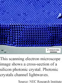
In nature, opals form spontaneously when millions of minute silica spheres stack up. The laboratory process and ingredients for artificial gemstone formation are the same. But to make a photonic bandgap opal, the researchers inverted the gemstone process, replacing the spheres with space and the gaps between the spheres with silicon. "By filling the space between the spheres with a semiconductor and then selectively removing the spheres, [we made] an extremely porous material," said Norris.
The researchers formed the inverted opals directly on a silicon wafer; they resemble honeycombs with thousands of round, rather than hexagonal, cells.
The process is tricky because the spherical spaces must be precise in order to form a photonic bandgap. In order to trap the light used in telecommunications networks, the inverted opals had to contain spherical spaces about one micron in diameter, which is one fifth the size of a red blood cell. A micron is one thousandth of a millimeter.
Though the particles used to make the spaces are microscopic, smaller particles are actually easier to work with. Previous attempts at making inverted photonic bandgap opals have been unsuccessful because it is difficult to position these 1-micron spheres precisely enough. The researchers solved the problem by making the spheres flow in a temperature-induced current, which kept the spheres mobile as they settled into their crystal formation.
The work is a clever demonstration that self-assembled crystals of spherical particles can be ordered into nearly defect-free structures, said Vincent Crespi, an associate professor of physics at Pennsylvania State University.
In order to allow optical materials to channel and guide light like the guiding of electrical signals in regular circuits, they require a high degree of perfection, Crespi said. "Through a clever induction of convective motion in the fluid that supports the assembling particles, the [researchers] keep these relatively large particles mobile enough to find their optimal positions in the growing crystal," he said.
Because the material is self-assembled, it is potentially much cheaper to make than today's computer chips, which require "extremely expensive lithographic equipment," said Crespi. Lithography uses a combination of chemicals and light to etch lines into silicon.
The crystal films seem to be of high quality, said Kai-Ming Ho, a professor of physics at Iowa State University. "Many groups have tried to make these inverse-opal photonic crystals, but usually the crystals have so many defects that only [a] pseudogap appears," he said. The researchers crystals contain a true, three-dimensional bandgap, he said.
The fabrication process is inexpensive and manufacturers should be able to use it to make the devices in volume, said Norris. The researchers' next step is to use the photonic bandgap crystals in a practical device. "We still have a long way to go with our approach," he said. It will be five or six years before the field of photonic bandgap materials in general has a practical impact, he added.
Norris's research colleagues were Yurii Vlasov at NEC and James Sturm and Xiang-Zheng Bo at Princeton University. They published the research in the November 15, 2001 issue of the journal Nature. The research was funded by NEC Corporation.
Timeline: 5-6 years
Funding: Corporate
TRN Categories: Materials Science and Engineering; Optical Computing; Optoelectronics and Photonics
Story Type: News
Related Elements: Technical paper, "On-Chip Natural Assembly of Silicon Photonic Bandgap Crystals," Nature, November 15, 2001.
Advertisements:
December 5, 2001
Page One
Nerve-chip link closer
Inside-out gem channels light
Computer follows video action
Environment may dictate intelligence
Physics methods may spot intruders
News:
Research News Roundup
Research Watch blog
Features:
View from the High Ground Q&A
How It Works
RSS Feeds:
News
Ad links:
Buy an ad link
| Advertisements:
|
 |
Ad links: Clear History
Buy an ad link
|
TRN
Newswire and Headline Feeds for Web sites
|
© Copyright Technology Research News, LLC 2000-2006. All rights reserved.