Molecule
chip demoed
By
Eric Smalley,
Technology Research NewsResearchers at Hewlett-Packard's HP Labs have made a working, 64-bit memory device that uses as few as a thousand molecules to store each bit of information, and they have come up with a process for mass-producing the molecular memory chip.
The researchers' prototype holds 10 times the data of a comparably-sized segment of a silicon memory chip. Ultimately, the molecular technology could pack 100 billion bits into a square centimeter of chip space, which is about 1,000 times what today's chips hold, according to Philip Kuekes, a computer architect at HP Labs.
The researchers have also made simple molecular logic circuits, and the technology could eventually be used to make entire computer processors, according to Kuekes.
HP's molecular technology could enable manufacturers to continue to make smaller chip components when silicon technology reaches its size limits in about 10 years, said Kuekes. Silicon computer chips have doubled in performance about every 18 months for the past 30 years, a phenomenon known as Moore's Law, because manufacturers have been able to make transistors and other components smaller. The photolithography processes used to make those components are likely to hit physical limits in about a decade.
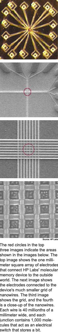
The molecular memory device consists of two sets of eight parallel wires arranged perpendicularly, one set on top of the other, to form 64 junctions. Each wire is 40 nanometers in diameter, or about 130 atoms across. Between the sets of wires is a layer of material only one molecule thick. "There's only about a thousand molecules in between two of those wires," said Kuekes.
Previous research has demonstrated electronic switches made from single molecules. HP's 1,000-molecule switches, however, are contained in a memory chip made in a scalable, relatively inexpensive manufacturing process. Theoretically, only a single molecule is needed to store each bit in the HP device.
The molecules act as minuscule electronic switches. Sending a pulse of electricity from one wire to another through the layer of molecules changes the molecules' resistance to the flow of electricity. These higher and lower resistance states can represent the ones and zeros of digital information.
A computer would write data to the memory by sending electrical pulses to specific junctions to change the resistance of the molecules there. The computer could then read the memory by using weaker electrical pulses that don't change the molecules' resistance but pass through a junction if the resistance is low and do not if it is high. The memory is nonvolatile, meaning it retains data even when the power has been turned off.
The molecular memory prototype contains a logic device and memory in a single, integrated circuit, said Kuekes. "We were able to build very simple logic [circuit], a demultiplexer, which is used to address a memory," he said. A demultiplexer channels signals from the memory device's wires through a smaller number of larger wires that connect the device to the outside world.
The molecular memory architecture could eventually be used to build more complicated logic circuits like those used to manipulate data in computer processors, according to Kuekes.
Perhaps more important than the prototype is the nanoimprint lithography process used to make it. "With this one manufacturing technology [we will] at some point be able to reinvent the integrated circuit, and build all the memory functions and logic functions that people are familiar with today," said Kuekes.
Nanoimprint lithography is a microscopic stamping technique that can inexpensively make many of the memory devices at a time, said Kuekes. The researchers made 625 of the prototype memory devices at once.
To make the stamp, the researchers carved a microscopic pattern of 625 sets of eight parallel 40-nanometer ridges on a block of silicon using an electron beam. Electron beams can be focused more narrowly, and so carve smaller patterns, than the laser beams used to make today's computer chips. "While it's fairly expensive and difficult to make a master, once you've got the master you can print out a large number of copies," said Kuekes.
The researchers pressed the stamp into a layer of plastic to make sets of eight parallel trenches, which they filled with platinum to make wires. Then they spread a layer of molecular switches on top of the wires. Next they deposited another layer of plastic, pressed the stamp into it perpendicularly to the first set of wires, and filled those trenches to make the second set wires. Last, they chemically removed the plastic, leaving the crossed wires sandwiching the molecular switches.
The HP prototype is a significant development, said Deepak Srivastava, a senior scientist and task leader at NASA Ames Research Center. "All the contributing technologies are scalable." The process could be used in commercial manufacturing plants within the next few years, he said.
High-density memories are likely to be among the first commercialized products to result from nanotechnology research, Srivastava added.
The researchers plan to make a memory device within three years that can store 16,000 bits in a 128-by-128 array of wires, said Kuekes. "We expect... to be both increasing the number of wires and decreasing the pitch between the wires," he said. Decreasing the pitch, or space, between the wires would allow the researchers to fit more wires, and therefore more junctions, in the same space.
The technique could be used to make useful memory devices in five to ten years, said Kuekes. It will take at least ten years of development before technique can be used to make other types of computer chips, he said.
Kuekes' research colleagues were R. Stanley Williams, Yong Chen, Douglas Ohlberg, Xuema Li, Duncan Stewart, Tan Ha, Gun-Young Jung and Hylke Wiersma. Williams presented the research at a symposium marking the 175th anniversary of the Royal Institute of Technology of Sweden. The research was funded by the Defense Advanced Research Projects Agency (DARPA) and Hewlett-Packard.
Timeline: 5-10 years
Funding: Government, Corporate
TRN Categories: Biological, Chemical, DNA and Molecular Computing; Integrated Circuits; Data Storage Technology; Nanotechnology
Story Type: News
Related Elements: None
Advertisements:
September 18/25, 2002
Page One
Molecule chip demoed
Diamond electronics on deck
Huge lasers could spark fusion
Diamonds improve quantum crypto
Software agents ask for help
News:
Research News Roundup
Research Watch blog
Features:
View from the High Ground Q&A
How It Works
RSS Feeds:
News
Ad links:
Buy an ad link
| Advertisements:
|
 |
Ad links: Clear History
Buy an ad link
|
TRN
Newswire and Headline Feeds for Web sites
|
© Copyright Technology Research News, LLC 2000-2006. All rights reserved.