Stamp
corrals tiny bits
By
Kimberly Patch,
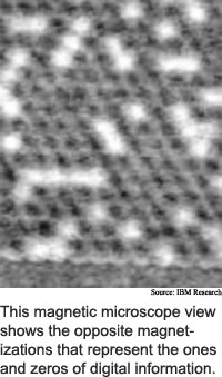
Technology Research NewsThe way disk drives store information in a computer is fairly straightforward -- microscopic areas of magnetic material represent 1s or 0s depending on their magnetic orientations. The smaller these magnetic areas, or bits, the more 1s and 0s fit on a disk.
One way to get more information on a disk is to make bits smaller. Disk drive manufacturers have managed to double the capacity of drives every year for the past five years, largely by shrinking bits. The laws of physics, however, are closing in. Today's densest prototype disk drives contain 100 gigabits, or billion bits per square inch; it looks like bits will not hold their magnetic orientations reliably beyond 200 gigabits per square inch.
This is because heat causes the magnetic grains that make up a bit to randomly flip their orientations; when a bit contains contain too few grains of material, enough grains can randomly flip that it becomes unclear whether the bit represents a 1 or a 0. "If the grains are made much smaller... the energy required to flip their magnetization can be so low that the magnetization would be thermally unstable," said Gary McClelland, a research staff member at IBM's Almaden research center.
The surfaces of today's standard disk drives are thin films of magnetic material, and individual bits are defined only by the actions of the recording head. It has been known for years that patterning, or physically isolating the magnetic material in each bit is one way to keep small numbers of grains aligned.
It takes extra work, however, to make specific patterns on the disks. Existing techniques are an estimated two to four orders of magnitude more expensive than today's disk manufacturing processes, said Robert White, a professor of electrical engineering and materials science at Stanford University and founder of the school's Center for Research on Information Storage Materials.
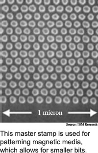
McClelland and his Almaden colleagues have found a way to stamp magnetic material onto a disk, and the method shows promise as a relatively inexpensive way to pattern media.
The researchers used beams of electrons to etch a master stamp, then spread a thin film of liquid polymer, or plastic, on a silicon oxide wafer. They pressed the stamp into the polymer using 290 pounds per square inch of pressure for a full minute, and at the same time hardened the polymer with ultraviolet light. The researchers then pressed the mirror image into a second layer of polymer on a wafer to form an exact replica of the stamp in plastic.
The process left a pattern of 28-nanometer-high polymer pillars. The researchers used a beam of electrically charged fluoride atoms to carve the polymer pattern into the underlying silicon oxide, then added several layers of magnetic film over the silicon oxide pillars.
One key to the process was making the stamp flexible. "By using a flexible stamp, we can accommodate the small but inevitable surface roughness and curvature present in glass disk substrates," said McClelland.
The tricky part of the process was finding the right mix of adhesion and release layers, McClelland said. The problem is one familiar anyone who's struggled to remove a recalcitrant cupcake from a tin -- the polymer had to stick to the glass surface, but not to the stamp. The design the researchers came up with enabled the polymer "to adhere to the glass substrate, but also allowed the stamp to separate easily," from the finished surface, McClelland said.
The researchers have managed to put together a process that many people have been talking about for a long time, said Stanford University's White. "It is significant that this comes out of IBM, [which] has the potential to utilize it," he said.
The Almaden technique is somewhat unusual because the magnetic layer was added at the end of the process, said White. "It isn't obvious that this would work," he said.
Although the idea of using imprint lithography has been around for about five years, and the use of flexible plates is also not unique, the researchers have managed to stamp out a relatively large area, which is also an important step, he said. "Because you can't use a step-and-repeat technique with this kind of resolution, you have to do it all in one slam dunk," he said.
The technique is also relatively simple, and thus potentially inexpensive, said White. "It's not dirt cheap, but it is a step toward an inexpensive way of making patterned media," he said. "Once you have the master you can make large numbers of copies."
The areal density of the researcher's prototype is 74 gigabits per square inch, which is about twice the density of existing commercial drives, said McClelland. It is feasible, however, to make patterns as dense as 500 gigabits per square inch using the technique, he said.
This type of technique could eventually push disk drive density as high as 2,000 gigabits, or 2 terabits per square inch, said White. Meanwhile, existing non-patterned media is likely to top out at 200 gigabits per square inch, he said.
The researchers are working on stamping out smaller bits, and also on using a standard disk substrate instead of the silicon oxide surface they used in their prototype, according to McClelland. Another step is figuring out how to write and read the bits at the high speeds today's disk drives require. "The major additional complication is the need to synchronize data writing and reading... as the disk rotates at high speeds," McClellan said.
Once the disk substrate is patterned by imprinting, the disk can probably be coated and finished using existing manufacturing processes, said McClelland.
It is premature to speculate about when any particular density-enhancing technology will be adopted by disk drive manufacturers, said McClelland. However, "if our research continues on its successful path, we expect that patterned media could be considered for adoption in about five years," he said.
Meanwhile, IBM rival Seagate is betting on a different horse. Instead of imposing a pattern on disk media, they're working on processes that will automatically build a pattern from the ground up. "Seagate is more actively pursuing self-ordered magnetic arrays as a means to achieving bit-patterned media," said Mark Kryder, a professor of electrical and computer engineering at Carnegie Mellon University, and Seagate's senior vice president of research.
Seagate's technology, dubbed heat assisted magnetic recording, combines self-ordered arrays of iron-platinum particles, which are very stable, with a technique that calls for heating the media with a laser beam to make it possible to write data to them. The technique could eventually lead to storage densities as high as 50 terabits per square inch, according to Seagate. Seagate's effort is partly funded by the U.S. Department of Commerce.
McClelland's research colleagues were Mark W. Hart, Charles T. Rettner, Margaret E. Best, Kenneth R. Carter, and Bruce D. Terris. They published the research in the August 19, 2002 issue of Applied Physics Letters. The research was funded by IBM.
Timeline: 5 years
Funding: Corporate
TRN Categories: Data Storage Technology; Materials Science and Engineering
Story Type: News
Related Elements: Technical paper, "Nanoscale Patterning of Magnetic Islands by Imprint Lithography Using a Flexible Mold," Applied Physics Letters, August 19, 2002.
Advertisements:
October 16/23, 2002
Page One
Chemists brew tiny wires
Voiceprints make crypto keys
Stamp corrals tiny bits
Net devices arranged fractally
Quantum scheme lightens load


News:
Research News Roundup
Research Watch blog
Features:
View from the High Ground Q&A
How It Works
RSS Feeds:
News
Ad links:
Buy an ad link
| Advertisements:
|
 |
Ad links: Clear History
Buy an ad link
|
TRN
Newswire and Headline Feeds for Web sites
|
© Copyright Technology Research News, LLC 2000-2006. All rights reserved.