Microfluidics make flat screens
By Eric Smalley, Technology
Research NewsAs flat-panel displays get bigger, the combination of complicated manufacturing equipment like vacuum deposition chambers and the increased chances of defects, given the larger screen areas, significantly boosts the cost of making the silicon backplanes that power the screens.
Backplanes that use organic, or plastic, transistors have the potential to be much easier and less expensive to produce. But existing methods of making organic transistors, which include photolithography processes similar to chipmaking techniques, screenprinting, and inkjet printing, have shortcomings ranging from expense to imprecision.
Researchers from the Palo Alto Research Center have turned to a technology used in biochips to overcome these problems. The researchers are using microfluidic devices, which contain tiny channels that control the flow of small amounts of fluids, to form organic transistors.
The process precisely aligns the polymer that makes up the bulk of the transistor with metal electrodes, and further simplifies organic manufacturing by allowing a semiconductor to be deposited and patterned in a single step, said Michael Chabinyc, a research scientist at the Palo Alto Research Center.
The polymeric thin film transistors could lead to inexpensive large-area flat-panel computer displays. The flexible transistors could also make foldable electronic paper backplanes possible.
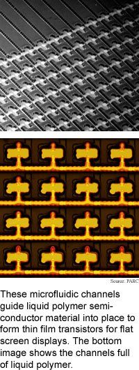
The researchers made an organic backplane prototype by printing a pattern of wax on a metal-coated transparent surface to define an array of circuits, then chemically removing metal left uncovered by the wax. They coated the surface with a photocurable polymer and shined ultraviolet light from the bottom to cure the polymer. The metal circuits blocked the light, which left the polymer above the circuits uncured. They washed away the uncured polymer to make channels directly aligned above the circuits. Once this mold was made, the researchers formed transistors by depositing liquid polymer semiconductor material into the channels and letting it dry in place.
Key to the simplicity of the manufacturing process is that it uses a passive fluid control process. Putting the liquid polymer semiconductor in place required no force because "the microfluidic channels act as a wick to draw the solution containing the polymer semiconductor across the array," said Chabinyc.
The researchers made microchannels that were 40 microns wide and 20 microns high. The pixel areas were 300 microns across. A micron is one-thousandth of a millimeter.
The performance of transistors made using the process is comparable to organic thin-film transistors made using existing methods, said Chabinyc. But the process is simpler than other techniques, he said.
The method does not require semiconductor materials that are engineered to handle the harsh conditions of the photolithography processes used to make thin film transistors, according to Chabinyc. It can also produce smaller structures than those made by screenprinting, and avoids the problem of controlling the spread of inkjet droplets, according to Chabinyc.
The researchers' approach also avoids vacuum processing. Small-molecule organic semiconductors are usually deposited onto a backplane surface using vacuum coating techniques to make thin-film transistors. Because the researchers use a polymer semiconductor that can be dissolved in a solvent, "the method... can be done in the ambient environment; thus the commercialization of the process should be less expensive," said Chabinyc. The process can be used to pattern any semiconductor material that can be dissolved, he said.
Using a microfluidic process to form electronics is not a new concept. Researchers have used patterned rubber stamps pressed against surfaces as molds to make circuits. But the stamp method has its drawbacks, including air bubbles, the difficulty of aligning the stamp with features on the surface, and the difficulty of filling the channels without depositing excess material on the surface, according to Chabinyc.
Polymer thin film transistors could be used in large-area displays and electronic paper in five to ten years, said Chabinyc. "There's much work to be done to improve the lifetime and environmental stability of organic devices before they can be commercialized," he said.
Chabinyc's research colleagues were W. S. Wong, K. E. Paul and Robert Street. The work appeared in the November 17, 2003 issue of Advanced Materials. The research was funded by the National Institute of Standards and Technology. The researchers also received samples from Dow Chemical Company and Xerox Research Center of Canada.
Timeline: 2 years
Funding: Government
TRN Categories: Integrated Circuits; Materials Science and Engineering; Microfluidics and BioMEMS
Story Type: News
Related Elements: Technical paper, "Fabrication of Arrays of Organic Polymer Thin-Film Transistors Using Self-Aligned Microfluidic Channels," Advanced Materials, November 17, 2003
Advertisements:
December 17/24, 2003
Page One
PDA translates speech
Device guards Net against viruses
Body handles nanofiber
Microfluidics make flat screens
Briefs:
Chemists grow nano menagerie
Solid fuel cell works in heat
Hybrid crypto secures images
Chip uses oil to move droplets
Light spots sort particles
Organic transistors get small

News:
Research News Roundup
Research Watch blog
Features:
View from the High Ground Q&A
How It Works
RSS Feeds:
News
Ad links:
Buy an ad link
| Advertisements:
|
 |
|
TRN
Newswire and Headline Feeds for Web sites
|
© Copyright Technology Research News, LLC 2000-2011. All rights reserved.