Ultrathin carbon speeds circuits
By
Eric Smalley,
Technology Research NewsWith silicon chipmaking technology facing the end of its viability in a decade or so, scientists are looking for alternative computer chip materials. One promising candidate is the carbon nanotube.
Nanotubes are rolled-up sheets of carbon atoms that have useful electrical properties and that can be smaller than one nanometer in diameter. They are ready-made circuit components, and researchers routinely fashion transistors from them. Researchers are a long way from being able to precisely arrange millions of nanotube transistors to form logic circuits on computer chips, however.
Researchers from the University of Manchester in England and the Institute for Microelectronics Technology in Russia have found that the equivalent of unrolled carbon nanotubes -- sheets of carbon atoms only a few atoms thick -- have comparable electrical properties and are more compatible with today's chipmaking methods.
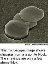
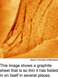
The molecular structure of one-atom-thick carbon sheets causes the sheets to roll up; tubular and spherical carbon molecules are common in nature. The researchers were able to peel ultrathin layers of graphite from graphite blocks to produce graphite sheets that are less than a nanometer thick and 10,000 nanometers wide.
The researchers used an ultrathin graphite sheet as the semiconducting channel of a transistor. They positioned a graphite sheet on an insulating layer of silicon oxide that sat on a silicon substrate, and connected source and drain electrodes to the sheet. Unlike bulk graphite, the ultrathin graphite's electrical conductance is changed by an electric field produced by a voltage applied to the silicon.
Depending on whether the voltage is positive or negative, the electric field increases the concentration of positive charge carriers -- holes -- or negative charge carriers -- electrons -- in the ultrathin graphite, making it more conductive to like charge carriers and more resistive to opposite charge carriers. This field effect is the basis of most transistors.
Transistors made from the ultrathin graphite sheets have the potential to be much faster than today's transistors made from semiconductors because the arrangement of atoms in the ultrathin graphite sheets causes electrons to travel through the sheets ballistically, or straight through, rather than bouncing off of the edges of the graphite channel, said Andre Geim, a professor of condensed matter physics at the University of Manchester in England. In today's electronics, electrons scatter in all directions as they travel within wires and circuits.
The ultrathin graphite sheets showed ballistic electronic transport over distances of nearly one micron, said Geim. "This distance is more than enough to make ballistic transistors," he said.
Charge carrier mobility is a measure of how readily negatively-charged electrons and positively-charged holes move through a material, which is a major factor in how efficiently a material conducts electricity. The sheets' carrier mobility is 10,000 square centimeters per volt second, according to Geim. In contrast, the silicon crystal used to make computer chips has a carrier mobility of 1,500 square centimeters per volt second.
Ballistic transistors are a holy grail for electronic engineers, said Geim. But ballistic transport is difficult to achieve in traditional electronic materials, typically requiring wires only a few atoms wide or temperatures close to absolute zero. "It is doubtful that any of the standard semiconductors -- silicon, gallium arsenide -- could lead to ballistic devices," he said.
Ultimately, the ultrathin graphite sheets could be made into wafers of the same area as the silicon wafers used today to make computer chips, according to Geim. Industrial silicon wafers can be as large as 30 centimeters in diameter. The wafers could then be processed into computer chips using today's photolithography chipmaking techniques.
In a related development, researchers at the Georgia Institute of Technology have devised a method for growing ultrathin graphite films by depositing a vapor of carbon atoms on a silicon-carbon crystal surface. The Georgia Tech researchers have made films three atoms thick and several millimeters wide.
Ultrathin graphite could be used practically within five years, said Geim.
Geim's research colleagues were Konstantin Novoselov, Da Jiang, Y. Zhang and Irina Gregorieva of the University of Manchester, and S. V. Morozov, S. V. Dubonos and A. A. Firsov of the Institute for Microelectronics Technology. They published the research in the October 22, 2004 issue of Science. The research was funded by the UK Engineering and Physical Sciences Research Council and the Russian Academy of Sciences.
The Georgia Tech researchers were Claire Berger, Zhimin Song, Tianbo Li, Xuebin Li, Asmerom Y. Ogbazghi, Rui Feng, Zhenting Dai, Alexei N. Marchenkov, Edward H. Conrad, Phillip N. First and Walt A. de Heer. They described their work in a paper posted on the arxiv physics archive at arxiv.org/abs/cond-mat/0410240.
Timeline: <5 years
Funding: Government
TRN Categories: Materials Science and Engineering; Integrated Circuits
Story Type: News
Related Elements: Technical papers "Electric Field Effect in Atomically Thin Carbon Films," Science, October 22, 2004; "Ultrathin Epitaxial Graphite: 2D Electron Gas Properties and a Route toward Graphene-Based Nanoelectronics," posted on the arxiv physics archive at arxiv.org/abs/cond-mat/0410240
Advertisements:
November 3/10, 2004
Page One
Ultrathin carbon speeds circuits
DNA machines take a walk
DNA in nanotubes sorts molecules
Single field shapes quantum bits
Briefs:
Nanotubes lengthen to centimeters
Coated nanotubes record light
Photonic crystal lasers juiced
Lasers move droplets
Molecules form nano containers
Square rings promise reliable MRAM
News:
Research News Roundup
Research Watch blog
Features:
View from the High Ground Q&A
How It Works
RSS Feeds:
News
Ad links:
Buy an ad link
| Advertisements:
|
 |
Ad links: Clear History
Buy an ad link
|
TRN
Newswire and Headline Feeds for Web sites
|
© Copyright Technology Research News, LLC 2000-2006. All rights reserved.