Ribbons expand nanotech toolbox
By Eric Smalley, Technology Research NewsResearchers are producing a range of new materials these days that form interesting shapes in microscopic sizes. The shapes, which include soccer balls, tubes, cylindrical wires and polyhedrons, determine many of the materials' properties, and are ready-made components for nanotechnology.
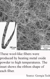
A team from the Georgia Institute of Technology has added a new shape -- ribbons. The researchers heated metal oxide powders and the resulting crystals formed in long, flat fibers. The ribbons are transparent and semiconducting.
The ribbons could find a wide range of applications, from smart windows and flat-panel displays, to transistors and diodes, to chemical sensors.
Smart windows using the ribbons could, for example, change the amount and type of light they allow to pass through based on temperature, keeping heat inside during winter and outside in summer. And like other semiconductors, the ribbons can be doped to be positively or negatively conducting and thereby become microelectronic components. The ribbons could also be used as sensitive chemical sensors because their conductivity changes when a relatively small number of molecules stick to their surfaces.
The researchers produced the ribbons by evaporating metal oxide powders at temperatures of 1,000°C or 1,400°C depending on the type of oxide. The process left a fuzzy material with individual ribbon-shaped fibers measuring several tens of microns to several millimeters in length.
The researchers made the ribbons using zinc oxide, tin oxide, indium oxide and cadmium oxide. The ribbons range from 50 to 500 nanometers wide and are 5 to 10 times as wide as they are thick. With the exception of some of the indium oxide ribbons, which sported narrower sections, the ribbons' width is uniform. The widest of these ribbons is half the width of an E. coli bacterium.
The ribbons are defect-free, single crystals that are perfectly flat, said Zhong Lin Wang, a professor of materials science and engineering at Georgia Tech. Cylindrical semiconductor nanowires, in contrast, are not flat at the atomic level, he said. The ribbons are also hardier then semiconductor nanowires, he said.
"If you look at other semiconductor nanowires, for example silicon, germanium or gallium arsenide, they always have a very thin layer of oxide on the surface because those materials are very sensitive to the atmosphere," said Wang.
Oxygen is very reactive, bonding with many other elements it comes into contact with two form oxides. Rust, for example, is iron oxide. Because the ribbons already contain oxygen they can't be oxidized any further, Wang said. "This means if you make a device from [the ribbons] it can work in any environment," he said.
The ribbons have a couple of advantages over carbon nanotubes, according to Wang. Carbon nanotubes can be either metal or semiconducting but currently they cannot be reliably produced in only one form or the other, while the ribbons are all semiconducting, he said.
It's also difficult to separate nanotubes from graphite particles because they are made of the same element. The best researchers have done to date is to achieve 70 percent purity for carbon nanotubes while the oxide ribbons are more than 95 percent pure, said Wang.
Carbon nanotubes have been studied extensively for the last ten years but metal oxides are just beginning to get attention, Wang said. "Any metal can make an oxide so the applications are enormous and the variety of structures [is] enormous. We really haven't taken advantage of this," he said.
The ribbons have interesting optical properties and will likely be good building blocks for nanoscale optoelectronics, said Peidong Yang, an assistant professor of chemistry at the University of California in Berkeley. "Wang's work is interesting... a simple thermal evaporation method to produce nanowires with rectangular cross-section. The method seems quite general," he said.
"How... the geometry of nanowire cross-section [effects the wires'] physical properties remains unknown at this point and should be a highly interesting issue to address," said Yang.
The first practical applications for the semiconducting oxide ribbons will likely be chemical sensors and these could be developed in three to five years, said Wang.
Wang's research colleagues were Zheng Wei Pan and Zu Rong Dai. They published the research in the March 9, 2001 issue of Science. The research was funded by the National Science Foundation.
Timeline: 3-5 years
Funding: Government
TRN Categories: Semiconductors and Materials; Nanotechnology
Story Type: News
Related Elements: Technical paper, "Nanobelts of Semiconducting Oxides," Science, March 9, 2001
Advertisements:
March 14, 2001
Page One
Tools cut data down to size
Ribbons expand nanotech toolbox
Silicon cages metal atoms
Surfaces channel liquids
Chip impurities make quantum bits
News:
Research News Roundup
Research Watch blog
Features:
View from the High Ground Q&A
How It Works
RSS Feeds:
News
Ad links:
Buy an ad link
| Advertisements:
|
 |
Ad links: Clear History
Buy an ad link
|
TRN
Newswire and Headline Feeds for Web sites
|
© Copyright Technology Research News, LLC 2000-2006. All rights reserved.