Spot
of gold makes tiny transistor
By
Chhavi Sachdev,
Technology Research NewsMaking faster computers means making smaller circuits in order to shorten the paths electrons follow. The smallest transistor possible would let only one electron pass through at a time, and could lead to computers that are much faster and require much less power than todays models.
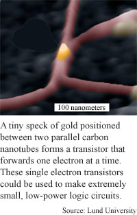
Researchers in Sweden and Denmark have found a way to use carbon nanotubes as electronic leads that connect a circuit with a tiny particle of gold to form a single-electron transistor.
The researchers transistor is a first step towards single-electron devices that would measure a mere 3 or 4 nanometers, or about as wide as 30 to 40 hydrogen atoms end to end. Single-electron transistors have to be this small in order to work at room temperature.
Manipulation of such tiny objects is a delicate process. The researchers managed to position a carbon nanotube between two electrodes using an atomic-force microscope (AFM) tip. Then they used the tip to cut the nanotube -- a rolled-up sheet of carbon atoms -- into two sections, "each section still in contact with its respective electrode," said Lars Samuelson, a professor of Solid State Physics and Head of the Nanometer Structure Consortium at Lund University. Next, the researchers made the nanotube halves parallel, and deposited a 7-nanometer gold nanoparticle between them.
The researchers then adjusted the temperature. They found that cooling the device below 200 degrees Kelvin, or -73 degrees Celsius, makes it an ideal single-electron transistor, said Samuelson.
The researchers next plan to use smaller nanoparticles to make a device that will operate at room temperature, said Samuelson.
This is good work, said Zhen Yao, an assistant professor of physics at the University of Texas at Austin. "This approach opens up [ways] to systematically study the electronic properties of individual nanoparticles --metallic, semiconducting, magnetic, or superconducting -- as a function of their sizes," he said.
This type of systematic study is crucial to testing nanoparticles for various applications but has been lacking mainly because it is difficult to address individual nanoparticles, Yao said. "They are typically 2 to 10 nanometers in diameter, which is beyond the resolution of standard electron-beam lithography" processes used to make experimental computer chips.
The method is useful for basic science but probably not for practical applications, said Hongkun Park, an assistant professor of Chemistry at Harvard University. AFM manipulation is not a practical strategy to make commercial devices, because it can only be used to make one device at a time, which is far too slow for manufacturing, he said.
Samuelsons research colleagues were Claes Thelander, Martin H. Magnusson, and Knut Deppert at Lund University in Sweden, and Per Rugaard Poulsen, Jesper Nygard, and Jorn Borggreen at the Niels Bohr Institute at the University of Copenhagen, Denmark. They published the research in the September 24, 2001 issue of the journal Applied Physics Letters. The research was funded by the Swedish Foundation for Strategic Research (SFF), The Swedish Research Council for Natural Sciences and for Engineering Sciences, and the European Union (EU).
Timeline:
Funding: Government
TRN Categories: Nanotechnology; Integrated circuits
Story Type: News
Related Elements: Technical paper, "Gold Nanoparticle Single-Electron Transistor With Carbon Nanotube Leads," Applied Physics Letters, September 24, 2001.
Advertisements:
November 21, 2001
Page One
Chemists create nano toolkit
English could snowball on Net
Page age shapes Web
Circuits show six degrees of separation
Spot of gold makes tiny transistor

News:
Research News Roundup
Research Watch blog
Features:
View from the High Ground Q&A
How It Works
RSS Feeds:
News
Ad links:
Buy an ad link
| Advertisements:
|
 |
Ad links: Clear History
Buy an ad link
|
TRN
Newswire and Headline Feeds for Web sites
|
© Copyright Technology Research News, LLC 2000-2006. All rights reserved.