Coax
goes nano
By
Eric Smalley,
Technology Research NewsWires that are structured like television cable but are a thousand times narrower than human hair could form the future of semiconductor technology.
Researchers at Harvard University have made microscopic wires from layers of different materials using the semiconductor manufacturing processes used to construct computer chips.
The layered wires are new building blocks for nanotechnology, according to Charles Lieber, a professor of chemistry at Harvard University. The vanishingly small nanowire components could be used to make faster computer chips, higher-density memory and smaller lasers.
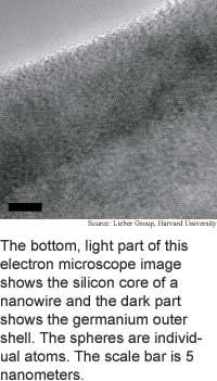
To form a 50-nanometer layered wire, the researchers started with a gold droplet a mere 20-nanometers across. A nanometer is one millionth of a millimeter; 20 nanometers is about the size of a line of 200 hydrogen atoms.
The researchers coaxed a semiconductor vapor to condense on one side of the gold droplet and form a nanowire of about the same diameter as the droplet.
They then caused additional layers of material to form around the wire by adjusting the manufacturing conditions, said Lieber. "This is actually quite easy," he said. "The surface area of the nanowire is much, much larger than that of the [droplet], and [layering] generally just involves... increasing the temperature or concentration" of the vapor.
Different vapors provide different materials. The researchers made several prototype wires, including a 50-nanometer-diameter nanowire made of a 19-nanometer core of pure silicon and a shell of silicon doped, or mixed, with boron. Semiconductors used in electronics are often doped to make them conduct electricity more readily.
The researchers also made several other types of nanowire: a 26-nanometer germanium core with a 15-nanometer doped silicon shell; a 21-nanometer doped silicon core with a 10-nanometer germanium shell; and a 20-nanometer silicon core with a 30-nanometer middle layer of germanium and an a 4-nanometer outer shell of doped silicon.
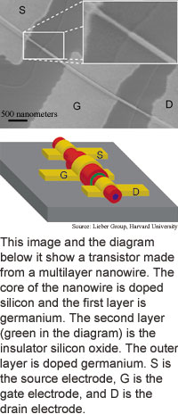
The researchers demonstrated the usefulness of the layered nanowire technique by using it to make a field-effect transistor. Transistors are the basic building blocks of computers and most other electronic devices.
A transistor consists of a channel that carries current, a source electrode that conducts current into the channel, a drain electrode that carries current away, and a gate electrode that turns on the transistor by increasing the electrical conductivity of the main channel, which allows current to flow through the device.
The researchers' built a transistor by layering 10 nanometers of germanium over a 10-nanometer doped silicon core, then adding a 4-nanometer layer of the insulator silicon oxide followed by a 5-nanometer outer layer of doped germanium. The researchers attached a gate electrode to the outer germanium layer, and source and drain electrodes to the inner germanium layer.
The researchers' prototype transistor is several times narrower than those used in today's computer chips.
The researchers used a similar technique last February to produce nanowire segments composed of different materials. Together, the segmenting and layering techniques will allow researchers to control nanowire composition along both length and width.
The work is "a major advance," said Zhong Lin Wang, a professor of materials science and engineering at the Georgia Institute of Technology.
Most nanoscale electronic devices made from carbon nanotubes or nanowires are oriented lengthwise, Wang said. The Harvard work shows for the first time that the different layers that make up field-effect transistors and other devices can be positioned across the width of nanowires, he said. "This research demonstrates the possibility of building much smaller devices based on nanowires," he said
The researchers have produced a "very nice piece of work" that clearly demonstrates the versatility and technical potential of heterostructure semiconductor nanowires, said Peidong Yang, an assistant professor of chemistry at the University of California at Berkeley. Yang led a research team that recently developed a similar technique to make ribbon-shaped nanoscale heterostructures, or structures made from two or more semiconductors. "Heterostructures are the common components for many of the electronic and optical devices in our daily lives, such as transistors, light-emitting diodes and laser diodes," he said.
The Harvard researchers are working on making a high-performance field-effect transistor that could be integrated with conventional electronic circuitry, said Lieber. "We are pushing very hard to make [a] transistor that could find its way into hybrid devices," he said. "This is something we're discussing with Intel's advanced transistor group."
The researchers are also using layered nanowires to construct a new type of nonvolatile random access memory, said Lieber. Nonvolatile memory retains data even when the power is turned off.
They are also looking to use the nanowires to make devices that produce light, including single-nanowire lasers, he said.
Before the nanowires can be used in practical applications, the growth process must be controlled more finely to produce more perfect structures, said Lieber.
Prototype nanowire transistors could be built in two to five years, said Lieber. The biggest technological hurdle is integrating these building blocks into useful devices, he said. "This is the same issue facing much of the field."
Lieber's research colleagues were Lincoln Lauhon, Mark Gudiksen and Deli Wang. They published the research in the November 7, 2002 issue of the journal Nature. The research was funded by the National Science Foundation (NSF), the Office of Naval Research (ONR) and the Defense Advanced Research Projects Agency (DARPA).
Timeline: 2-5 years
Funding: Government
TRN Categories: Nanotechnology; Integrated Circuits; Semiconductors; Materials Science and Engineering; Chemistry
Story Type: News
Related Elements: Technical paper, "Epitaxial core-shell and core-multishell nanowire heterostructures," Nature, November 7, 2002
Advertisements:
November 13/20, 2002
Page One
Coax goes nano
Webs within Web boost searches
Circuit gets more power from shakes
Method measures quantum quirk
Biochip sprouts DNA strands
News:
Research News Roundup
Research Watch blog
Features:
View from the High Ground Q&A
How It Works
RSS Feeds:
News
Ad links:
Buy an ad link
| Advertisements:
|
 |
Ad links: Clear History
Buy an ad link
|
TRN
Newswire and Headline Feeds for Web sites
|
© Copyright Technology Research News, LLC 2000-2006. All rights reserved.