Chip sorts colors
By
Eric Smalley,
Technology Research NewsThe simple concept of proportionality is the key to a significant advance in the emerging field of integrated optics -- chips that control light rather than electricity.
The field could lead to high-speed, all optical computers, and smaller, more efficient communications devices.
The photonic crystals that form integrated optics chips contain regularly spaced gaps that block certain wavelengths of light. The boundaries between the material and the gaps refract, or bend, light in the same way that the boundary between air and water produces the familiar bent-drinking-straw illusion.
By adding intentional defects, or areas without gaps, researchers can get photonic crystals to channel light through very small areas. It has been difficult, however, to make photonic crystals that efficiently handle several wavelengths, or colors, of light at once, said Susumu Noda, a professor of electronic science and engineering at Kyoto University.
Researchers at the university have discovered a design principle that overcomes this problem. They found that using several photonic crystals and making the size and spacing of the gaps in one crystal proportional to those in the next permits control of different wavelengths of a single beam of light. "We can expect to achieve multi-wavelength operation by simply connecting multiple photonic crystals with proportional unit-cell sizes," said Noda.
Previous attempts to control multiple wavelengths in photonic crystals solely through defects of different sizes have resulted in devices with poor performance, said Noda.
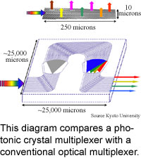
The Kyoto researchers used the method to make an add/drop multiplexer that is 250,000 times smaller than conventional optical multiplexors, said Noda. Add/drop multiplexers combine and separate different wavelengths in the same channel. The devices are widely used in communications networks; they increase network bandwidth by putting multiple signals over the same line at the same time.
The researchers' prototype device measures 250 microns by 10 microns; commercial devices are about 1 square inch, according to Noda. A micron is one thousandth of a millimeter.
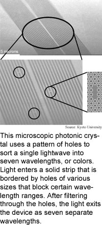
The researchers' add/drop multiplexer consists of a series of seven photonic crystals, each with a line defect to guide light through the crystal and a point defect to trap and emit photons, Noda said.
The device's success is due to proportionality: the distance from the center of one gap to the center of the next gets successively smaller, from 418.75 nanometers to 411.25 nanometers. Each crystal's gap spacing is 1.25 nanometers smaller than the previous one. A nanometer is the length of a row of 10 hydrogen atoms.
The device separates seven slightly different colors, or wavelengths, of the infrared light used for long distance communications over optical fibers. The wavelengths differ by five nanometer.
The field of two-dimensional in-plane photonic crystals is "very exciting right now," and the researchers' method appears to be capable of producing integrated optical devices, said Eli Yablonovitch, a professor of electrical engineering at the University of California at Los Angeles.
The method's advantage is simplicity, Yablonovitch said. "The main difference from previous work is in the simplicity of the design concept."
The researchers are working on a practical add/drop device, said Noda. The method could also be used for nonlinear optics and nanoscale biological sensors, he said.
The method could be used to produce practical devices in two to five years, said Noda.
Noda's research colleagues were Bong-Shik Song and Takashi Asano. They published the research in the June 6, 2003 issue of Science. The research was funded by Core Research for Evolution Science and Technology (CREST), Japan Science and Technology Corporation (JST), and the Japanese Ministry of Education, Culture, Sport, Science, and Technology.
Timeline: 2-5 years
Funding: Government
TRN Categories: Optical Computing, Optoelectronics and Photonics; Materials Science and Engineering
Story Type: News
Related Elements: Technical paper, "Photonic Devices Based on In-Plain Hetero Photonic Crystals," Science, June 6, 2003
Advertisements:
June 18/25, 2003
Page One
Chip sorts colors
Software referees group calls
Prefab key to molecular memory
Wires make wireless strain gauge
News briefs:
See-through circuits closer
Protein traps nanoparticles
Nods drive audio interface
Nano rapid prototyping advances
Practical nanotube fiber near
Nanotube transistors make memory
News:
Research News Roundup
Research Watch blog
Features:
View from the High Ground Q&A
How It Works
RSS Feeds:
News
Ad links:
Buy an ad link
| Advertisements:
|
 |
Ad links: Clear History
Buy an ad link
|
TRN
Newswire and Headline Feeds for Web sites
|
© Copyright Technology Research News, LLC 2000-2006. All rights reserved.