Atomic scopes eye living tissue
By
Eric Smalley,
Technology Research NewsThere's a lot to a butterfly's wing. Its barely visible scales are made from fragile, infinitesimal structures that underlie the insect's ability to perform a wide variety of precise maneuvers.
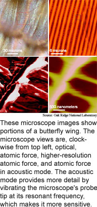
Researchers from Oak Ridge National Laboratory and North Carolina State University have used a scanning probe microscope to look at the structure of a butterfly's wing at a resolution of five nanometers, or two and a half times the width of DNA molecule. A nanometer is one millionth of a millimeter, or the span of 10 hydrogen atoms.
The pictures show individual chitin fibrils, making it possible to study the mechanical properties of the wing on the level of a single structural element. The pictures are a proof-of-concept that show that it is possible to use scanning probe microscopes to analyze material from living systems.
Scanning probe microscopy is usually used to examine inorganic materials like the ferroelectrics used in electronics, and organic materials like plastics. Scientists have also been able to use the instruments to study isolated biological molecules like DNA.
The ability to see living tissue at the molecular level will help scientists understand the properties of all kinds of biosystems, said Sergei Kalinin, a research and development staff member at the Oak Ridge National Laboratory. A better understanding of how living structures function could enable better artificial materials, assessments of disease, and drug and physical therapies, he said.
Scanning probe microscopes show information about the surface structure and electrical, magnetic, optical and mechanical properties of a material. The microscopes allow researchers to image tiny areas using friction, electricity, magnetism and acoustics.
Scanning probe microscopes consist of a microscopic tip attached to a tiny arm. The basic operation mode is to drag the tip across a sample and measure how much the arm is deflected, which reveals the sample's height at each point. Scanning in a series of lines creates a topographic image of the sample.
Material properties are measured using other modes, including current, which measures a sample's electrical conductivity; electrostatic, which measures the electrostatic interaction between the tip and the sample; magnetic, which measures the local magnetic field at each point on a sample; acoustic, which uses changes in vibration rates to measure elasticity; pulsed, which measures stickiness; and scanning coupling, which uses the quantum ability of electrons to jump across a gap to measure electrically conducting samples in atomic detail.
"We attempted to use several scanning probe microscope modes developed to study mechanical and electromechanical properties in... semiconductors," said Kalinin. "To our surprise, we found that using acoustic imaging allows imaging much finer details of the internal structure of... biological systems than we believed possible," he said.
The basic topographic image of the butterfly wing shows details down to about 100 nanometers, including the mesh structure that enables high mechanical stability and rigidity of the wing, said Kalinin. The acoustic imaging mode shows details down to five nanometers. This allows for the study of mechanical properties "on the level of single structural element forming the biological tissues -- chitin rods," he said.
The ultimate goal is to establish methods of using the microscope to qualitatively measure properties of biological tissue that are too small or too fragile to be studied by conventional testing, said Kalinin. "To be able to see and quantitatively measure, rather than guess, mechanical and electromechanical properties on the nanoscale can well hold the key for unraveling the origins of biological functionality in these materials," said Kalinin.
The researchers also want to push the technology to its limits. "We want to achieve maximally high resolution," said Kalinin. "Can we probe a single molecule inside [a] biological system?"
Possibilities include understanding the effects of hard tissue diseases like dental cavities and osteoporosis, and understanding tissue behaviors that could provide the basis for drug and physical therapies and methods of identifying cancer cells, said Kalinin. "We're interested in making our measurements quantitative, so we can say not only whether a particular region is softer or harder, but exactly how hard or soft it is," he said.
This is a very complex task that requires mathematical tools to describe tip-surface contact mechanics and a way to measure the shape of the tip, said Kalinin.
The researchers are exploring using scanning probe microscopes to study electrical and electromechanical interactions in biological tissues, which could provide insights into bone growth, muscular activities and other phenomena, said Kalinin. They are also working with other scientists to use scanning probe microscopy to study cell development and differentiation, he said.
It will be possible to take practical measurements of hard tissues like bones and teeth within several years, said Kalinin. Establishing guidelines for quantitative measurements and developing the appropriate calibration standards for those measurements will take longer, he said.
Kalinin's research colleague was Alexei Gruverman, an associate research professor of materials science at North Carolina State University. The research was funded by the Oak Ridge National Laboratory and the National Science Foundation.
Timeline: 1-5 years
Funding: Government
TRN Categories: Applied Technology
Story Type: News
Related Elements: None
Advertisements:
February 9/16, 2005
Page One
Atomic scopes eye living tissue
Brainwave interface goes 2D
Software ties marks to digital text
View from the High Ground:
Xerox's Hervé Gallaire
Briefs:
All-silicon chip laser demoed
Nanotubes crank out hydrogen
Nanotubes on plastic speed circuits
Lens design promises tight spots
Silicon nanocrystal transistor shines
Nano triangles concentrate light
Musical additions sound alarm
News:
Research News Roundup
Research Watch blog
Features:
View from the High Ground Q&A
How It Works
RSS Feeds:
News
Ad links:
Buy an ad link
| Advertisements:
|
 |
Ad links: Clear History
Buy an ad link
|
TRN
Newswire and Headline Feeds for Web sites
|
© Copyright Technology Research News, LLC 2000-2006. All rights reserved.